


 |
市場調查報告書
商品編碼
1438411
面板級封裝:市場佔有率分析、產業趨勢與統計、成長預測(2024-2029)Panel Level Packaging - Market Share Analysis, Industry Trends & Statistics, Growth Forecasts (2024 - 2029) |
||||||
※ 本網頁內容可能與最新版本有所差異。詳細情況請與我們聯繫。
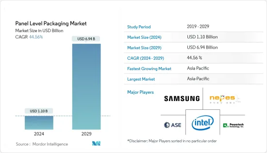
預計2024年面板級封裝市場規模為11億美元,預計2029年將達到69.4億美元,在預測期間(2024-2029年)年複合成長率為44.56%。
半導體產業正在經歷快速成長,半導體已成為所有現代技術的基本組成部分。該領域的進步和創新對所有下游技術產生直接影響,從而推動了市場研究的需求。
主要亮點
- 400mm 晶圓需求正在轉向面板級封裝。面板級封裝是晶圓層次電子構裝扇出之後的一步。世界各地的供應商都專注於擴展 PLP,而不是製定 450mm晶圓層次電子構裝的藍圖。此外,PLP 預計將透過並行化製程步驟並在矩形面板格式封裝(而不是圓形晶圓幾何形狀)中實現更高的面積利用率來提供顯著的成本效益,從而減少材料浪費。
- 然而,隨著封裝尺寸從晶圓到更大的面板格式的增加,此外,並行製造的封裝數量的增加,成本優勢導致向面板級封裝的轉變正受到越來越多的關注。此外,PLP 可以採用其他技術領域的製程、材料和設備。印刷基板(PCB)、液晶顯示器 (LCD) 和太陽能電池均以面板尺寸製造,提供了新的扇出面板級封裝方法。
- 此外,消費性電子和汽車等各種最終用戶行業的小型化趨勢也給封裝供應商帶來了越來越大的壓力。從覆晶到晶圓層次電子構裝的轉變是一個已經持續多年的趨勢。然而,下一類先進封裝正在從 300mm 晶圓級封裝轉向面板級封裝。
- 封裝製程有兩種類型:先模具和先 RDL。然而,晶片移位是這種類型封裝的一個問題。晶片移位被認為是最大的問題之一,因為它會降低產量比率或對產量比率產生負面影響。這增加了對包裝過程進行更好控制的需求並增加了複雜性。
- COVID-19大流行從需求和供應雙方影響了整個半導體製造市場。此外,全球半導體工廠停工或關閉加劇了供不應求。這種影響也體現在面板級封裝市場。然而,其中許多影響將是短期的。世界各國政府為支持汽車和半導體產業所採取的預防措施可能會重振產業成長。
面板級封裝市場趨勢
對小型、高性能電子設備的需求不斷成長,預計將佔據很大佔有率
- 消費性電子產品是市場上主要的最終用戶產業之一。智慧型手機產業的成長、智慧型裝置和穿戴式裝置的日益普及,以及消費者物聯網裝置在智慧家庭等應用中的普及不斷提高,是推動所研究細分市場成長的關鍵因素。
- 消費性電子產業的小型化趨勢正在創造更小、更輕、更可攜式的設備。消費性電子產品中的每一款新產品都比其前身更具創新性、更輕且更節能。這讓客戶對下一次迭代產生了很高的期望,使其成為家電生產商的關鍵賣點。先進的半導體封裝技術有助於滿足消費性電子市場複雜且不斷變化的需求。
- 由於對高性能、高能效、薄型和小尺寸封裝的需求,面板級封裝擴大用於智慧型手機等空間敏感型設備。因此,近年來這些設備的日益普及也為該市場創造了巨大的需求。例如,根據愛立信的數據, 年終智慧型手機相關合約數量為63億份,約佔行動電話合約總數的77%。這項預測預計到 2027 年訂閱量將達到 78 億,約佔所有行動電話訂閱量的 87%。
- 扇出面板級封裝 (FOPLP) 因其許多優點(包括低成本潛力)而在許多家用電子電器應用中穩步普及。目前,採用此技術的主流整合晶片包括用於5G智慧型手機的封裝天線(AiP)天線模組、用於穿戴式裝置的整合晶片以及物聯網(IoT)用例。
- 這樣,近期5G和物聯網的普及為市場帶來了顯著的成長機會。例如,根據GSMA的預測,2025年,5G網路預計將覆蓋全球三分之一的人口。該組織也預測,到年終年底,5G連線數將超過10億,到2025年將超過20億,佔行動連線的五分之一以上。
- 隨著5G投資的增加,對相容5G的智慧型手機的需求也隨之增加。例如,根據消費者技術協會(CTA)的數據,2022年5G智慧型手機的收益預計將達到613.7億美元,比2021年的533.8億美元成長15%。預計2021年5G智慧型手機將佔所有智慧型手機銷量的62%,2022年將上升至72%。
亞太地區預計將佔據較大佔有率
- 台灣因其強大的ICT產業基礎、堅實的半導體製造群和先進的製造能力而被譽為電子製造中心。這些優勢促進了許多提供先進ICT相關產品的本地公司的快速發展,主要集中在電子元件、電腦、光纖電纜和通訊設備領域。
- 該地區也受益於台積電和日月光等大型半導體公司的存在,這些公司專注於投資先進的半導體封裝解決方案。台積電已在台灣北部運作四家先進封裝工廠,分別位於新竹科學園區(HSP)、中央科學園區(CTSP)、南部科學園區(STSP)和龍塘。該公司目前計劃在台灣南部的嘉義市或雲林縣建立一座新的先進封裝工廠。
- 台灣最近宣布額外支出 2,369.6 億新台幣(85.6 億美元),用於在未來五年內採購武器,以應對中國的威脅。這筆獨特的預算預計將主要用於2022年至2026年購買本土武器系統。此類投資預計將進一步促進半導體元件的使用,從而對市場產生積極影響。
- 此外,日本的通訊市場也是全球收入最大的電信市場之一,儘管整體市場受到經濟和人口成長緩慢的支撐,但在過去二十年中,日本在鐵塔和光纖基礎設施方面投入了大量資金。固定/行動網路營運商。
- 汽車產業佔該國半導體零件總需求的很大一部分。此外,增加自動駕駛汽車採用的措施也進一步推動了市場成長。
面板級封裝產業概述
該市場主要由三星電子、英特爾公司、Nepes公司、日月光集團和PowerTech科技公司主導,這些公司在市場上佔有很大佔有率。然而,在未來幾年,我們預計將有更多的公司參與廣泛的研發和市場開拓活動,以開發有競爭力的面板級封裝技術。
- 2022 年 7 月 - Nepes 宣布將增加使用最先進的封裝技術之一——扇出面板級封裝 (FO-PLP) 進行量產的產品數量。電源管理積體電路(PMIC)之後將是轉碼器晶片和應用處理器。
- 2022 年 2 月-英特爾以每股 530 億美元現金收購 Tower Semiconductor。此次收購是英特爾IDM 2.0策略的重大進步,因為該公司進一步擴大了製造能力,擴大了封裝技術、全球足跡和技術組合,以滿足業界前所未有的需求。
其他福利:
- Excel 格式的市場預測 (ME) 表
- 3 個月分析師支持
目錄
第1章 簡介
- 研究假設和市場定義
- 調查範圍
第2章調查方法
第3章執行摘要
第4章市場洞察
- 市場概況
- 產業吸引力-波特五力分析
- 供應商的議價能力
- 買方議價能力
- 新進入者的威脅
- 替代品的威脅
- 競爭公司之間的敵對關係
- 產業價值鏈分析
- COVID-19 市場影響評估
第5章市場動態
- 市場促進因素
- 降低包裝過程成本
- 對小型和高性能電子設備的需求不斷成長
- 加大研發投入
- 市場限制因素
- 包裝工藝複雜
第6章市場區隔
- 按工業用途
- 消費性電子產品
- 車
- 通訊
- 其他工業應用
- 按地區
- 美國
- 中國
- 韓國
- 台灣
- 日本
- 歐洲
- 世界其他地區
第7章 競爭形勢
- 公司簡介
- Samsung Electronics Co. Ltd
- Intel Corporation
- Nepes Corporation
- ASE Group
- Powertech Technology Inc.
- Fraunhofer Institute for Reliability and Micro integration IZM
- Unimicron Technology Corporation
- DECA Technologies Inc.
- JCET/STATSChipPAC
第8章投資分析
第9章市場的未來
The Panel Level Packaging Market size is estimated at USD 1.10 billion in 2024, and is expected to reach USD 6.94 billion by 2029, growing at a CAGR of 44.56% during the forecast period (2024-2029).
The semiconductor industry is witnessing rapid growth, with semiconductors emerging as the basic building blocks of all modern technology. The advancements and innovations in this field directly impact all downstream technologies and drive the market study's need.
Key Highlights
- The need for 400 mm wafers is shifting focus toward panel-level packaging. Panel-level packaging is one of the following steps for Fan-out wafer-level packaging. Vendors across the globe are focusing on upscaling PLP instead of drawing a roadmap to 450 mm Fan-out Wafer Level Packaging. In addition, PLP is expected to offer significant cost advantages by parallelizing process steps and allowing higher area utilization of packages in rectangular panel formats rather than round wafer shapes to lower material waste.
- However, the focus on Panel Level Packaging is increasing due to the cost benefits and expanding the packaging size from wafer to larger panel formats and, in addition to that, increasing the number of packages manufactured in parallel. Additionally, PLP can adopt processes, materials, and equipment from other technology areas. Printed Circuit Board (PCB), Liquid Crystal Display (LCD), or solar equipment is manufactured on panel sizes and offers new Fan-out Panel Level Packaging approaches.
- Moreover, the constant trend of miniaturization across various end-user industries, such as consumer electronics, automotive, and others, has also increased pressure on packaging vendors. The transition from Flip-Chip to Wafer Level packaging has continued to be a trend for several years. However, the following type of advanced packaging is shifting from 300mm wafer-level packaging to Panel level packaging.
- The packaging process involves both types, Mold first and RDL first. However, the type of packaging involves problems in die shift. Die shifting is considered one of the biggest issues as it may cause lesser yield or negatively influence the yields. This increases the need for more control over the packaging process and adds complexity.
- The COVID -19 pandemic affected the overall semiconductor manufacturing market from the demand and supply sides. In addition, the global lockdowns and closure of semiconductor plants further fueled the supply shortage. The effects were also reflected in the Panel level packaging market. However, many of these effects are likely to be short-term. Precautions by governments across the globe to support automotive and semiconductor sectors could help revive industry growth.
Panel Level Packaging Market Trends
Increasing demand for compact, high functionality electronic devices is Expected to Hold Major Share
- Consumer electronics is one of the major end-user industries in the market. Growth in the smartphone industry, increasing adoption of smart devices and wearables, and increasing penetration of consumer IoT devices in applications like smart homes are significant factors driving the growth of the studied segment.
- The miniaturization trend in the consumer electronics industry has given rise to smaller, lighter, and more portable devices. Each new iteration of consumer electronics products is more innovative, lightweight, and energy-efficient than its predecessors. This creates enormous customer expectations for the next iteration, which is a significant selling point for the producers of consumer electronics. Advanced semiconductor packaging technologies can help meet the consumer electronics market's complex and evolving needs.
- Panel-level packaging has been finding increasing applications in footprint-sensitive devices, such as smartphones, owing to the requirement of high-performing, energy-efficient, thin, and small form factor packages. As such, the growing penetration of these devices in recent years also create considerable demand for the market. For instance, as per Ericsson, there were 6.3 billion subscriptions associated with smartphones at the end of 2021, accounting for about 77% of all mobile phone subscriptions. This forecast is expected to reach 7.8 billion in 2027, accounting for around 87% of all mobile subscriptions.
- The popularity of fan-out panel level packaging (FOPLP) has been rising steadily for many consumer electronic applications due to its many advantages, including low-cost potential. The current mainstream chips that use this technology for integration include Antenna-in-Package (AiP) antenna modules of 5G smartphones, integrated chips of wearable devices, and Internet of Things (IoT) use cases.
- As such, the increasing penetration of 5G and IoT in recent years presents significant growth opportunities for the market. For instance, as per GSMA, by 2025, 5G networks are expected to cover one-third of the world's population. The organization has also predicted that the number of 5G connections will surpass 1 billion by the end of 2022 and 2 billion by 2025, making up over a fifth of mobile connections.
- With the rising investments in 5G, the demand for 5G-enabled smartphones is also increasing parallelly. For instance, as per the Consumer Technology Association (CTA), the revenues from 5G smartphones are expected to reach USD 61.37 billion in 2022, up 15% from USD 53.38 billion in 2021. 5G smartphones were also estimated to make up 62% of all smartphone units in 2021 and rise to 72% in 2022.
Asia pacific is Expected to Hold Significant Share
- Taiwan is a well-known electronics manufacturing hub owing to its strong ICT industry base, robust semiconductor manufacturing clusters, and advanced manufacturing capacity. These advantages have contributed to the rapid development of many regional companies that offer advanced ICT-related products, primarily in the sectors of electronic components, computers, fiber optic cable, telecommunications equipment, etc.
- The region also benefits from the presence of large semiconductor companies like TSMC and ASE that are focusing on investing in advanced semiconductor packaging solutions. TSMC already operates four advanced packaging fabs, located in Hsinchu Science Park (HSP), Central Taiwan Science Park (CTSP), Southern Taiwan Science Park (STSP), and Longton in northern Taiwan. The company now aims to build a new advanced packaging plant in Chiayi or Yunlin county, southern Taiwan.
- Taiwan has recently declared an extra spending bill of TWD 236.96 billion (USD 8.56 billion) to procure weaponry over the next five years to counter the threats posed by China. This unique budget is expected to be used primarily to purchase indigenous weapon systems from 2022 to 2026. Such investments are expected to drive the usage of semiconductor components further, thereby positively impacting the market.
- Moreover, the Japanese telecommunications market is also one of the largest in the world by revenue, with few large fixed and mobile network operators that have invested heavily in towers and fiber infrastructure over the past two decades despite an overall market underpinned by low economic and population growth.
- The automotive industry accounts for a significant share of the country's total demand for semiconductor components. Also, the steps taken to increase the adoption of autonomous vehicles further drive the growth of the market.
Panel Level Packaging Industry Overview
The market is considered moderately competitive with major players such as Samsung Electronics, Intel Corporation, Nepes Corporation, ASE Group, and PowerTech Technology Inc. These companies have a major share of the market. However, more companies will be involved in extensive R&D and market development activities to develop competitive panel-level packaging technology in the coming years.
- July 2022 - Nepes announced that it would increase the number of products it produces in huge quantities utilizing fan-out-panel level packages (FO-PLP), one of the most advanced packaging techniques. Following the Power Management Integrated Circuit (PMIC), codec chips and application processors will be introduced to the market.
- February 2022 - Intel acquired Tower semiconductors for USD 53 billion per share in cash. The acquisition significantly advances Intel's IDM 2.0 strategy as the company further expands its manufacturing capacity, expand packaging technologies, global footprint, and technology portfolio to address unprecedented industry demand.
Additional Benefits:
- The market estimate (ME) sheet in Excel format
- 3 months of analyst support
TABLE OF CONTENTS
1 INTRODUCTION
- 1.1 Study Assumptions and Market Definition
- 1.2 Scope of the Study
2 RESEARCH METHODOLOGY
3 EXECUTIVE SUMMARY
4 MARKET INSIGHTS
- 4.1 Market Overview
- 4.2 Industry Attractiveness - Porter's Five Forces Analysis
- 4.2.1 Bargaining Power of Suppliers
- 4.2.2 Bargaining Power of Buyers
- 4.2.3 Threat of New Entrants
- 4.2.4 Threat of Substitutes Products
- 4.2.5 Intensity of Competitive Rivalry
- 4.3 Industry Value Chain Analysis
- 4.4 Assessment of the Impact of COVID-19 on the Market
5 MARKET DYNAMICS
- 5.1 Market Drivers
- 5.1.1 Reduced Cost of Packaging Process
- 5.1.2 Increasing Demand for Compact, High Functionality Electronic Devices
- 5.1.3 Increased Investment on Research & Development Activities
- 5.2 Market Restraints
- 5.2.1 Complexity in Packaging Process
6 MARKET SEGMENTATION
- 6.1 By Industry Application
- 6.1.1 Consumer Electronics
- 6.1.2 Automotive
- 6.1.3 Telecommunication
- 6.1.4 Other Industry Application
- 6.2 By Geography
- 6.2.1 United States
- 6.2.2 China
- 6.2.3 Korea
- 6.2.4 Taiwan
- 6.2.5 Japan
- 6.2.6 Europe
- 6.2.7 Rest of the World
7 COMPETITIVE LANDSCAPE
- 7.1 Company Profiles*
- 7.1.1 Samsung Electronics Co. Ltd
- 7.1.2 Intel Corporation
- 7.1.3 Nepes Corporation
- 7.1.4 ASE Group
- 7.1.5 Powertech Technology Inc.
- 7.1.6 Fraunhofer Institute for Reliability and Micro integration IZM
- 7.1.7 Unimicron Technology Corporation
- 7.1.8 DECA Technologies Inc.
- 7.1.9 JCET/ STATSChipPAC
8 INVESTMENT ANALYSIS
9 FUTURE OF THE MARKET
 2024-2028年全球高階半導體封裝市場
 2024-2032 年半導體封裝市場報告(按類型、封裝材料、技術、最終用戶和地區)
 3D TSV:重要課題的考察與市場的分析
 高密度實裝(MCM,MCP,SIP,3D-TSV):市場分析及技術趨勢
 2.5D 和 3D 半導體封裝 - 市場佔有率分析、產業趨勢與統計、成長預測(2024 - 2029)
 全球半導體封裝市場規模、佔有率、成長分析(按材料、按應用)- 2023-2030 年產業預測
 2024 年 3D 半導體封裝全球市場報告
 先進半導體封裝市場報告:2030 年趨勢、預測與競爭分析
 嵌入式晶片封裝市場報告:2030 年趨勢、預測與競爭分析
 面板級封裝報告:2030 年趨勢、預測與競爭分析