


 |
市場調查報告書
商品編碼
1404474
原子層沉積設備:市場佔有率分析、產業趨勢與統計、2024年至2029年成長預測Atomic Layer Deposition Equipment - Market Share Analysis, Industry Trends & Statistics, Growth Forecasts 2024 - 2029 |
||||||
※ 本網頁內容可能與最新版本有所差異。詳細情況請與我們聯繫。
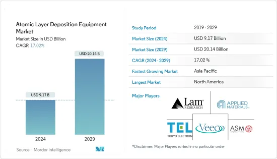
預計2024年原子層沉積設備市場規模為91.7億美元,預計2029年將達到201.4億美元,在預測期內(2024-2029年)複合年成長率為17.02%。
推動全球原子層沉積市場擴張的關鍵因素之一是全球擴大採用電子和半導體解決方案。
主要亮點
- 採用新材料和設計來提高晶片產量正在推動對原子層沉積解決方案的需求。小型化的趨勢正被世界各地的工業所擁抱。因此,對小型電子設備和機械的需求不斷增加。
- 據思科稱,到 2030 年,大約有 5,000 億台設備將連接到網路。每台機器都包含收集資料、與環境互動並透過網路通訊的感測器。這些應用需要小型化儲存設備和 IC。越來越多的連接設備產生的資料量不斷增加,增加了對儲存設備的需求並推動市場成長。
- 在半導體產業中,CMOS 處理器、儲存裝置、MEMS 和感測器中使用的高介電常數薄膜經常使用 ALD 來製造。 ALD 技術用於在燃料電池和其他需要耐腐蝕和耐磨的應用中創建功能性和保護性塗層。在下一代裝置的開發中,它們也被用於塗覆高長寬比結構,例如奈米線和奈米管。
- 多種沉積工具用於製造半導體,包括銅電極、高 k 閘極堆疊和銅阻擋層/籽晶層。例如,印度商工部下屬的國家投資促進和便利化管理局2022年3月發布的資料顯示,印度國內電子產品產量將從2014-15年的290億美元成長到2020-2021年。670億美元。
- 此外,機器人的使用和製造自動化的增加預計將增加半導體銷售並推動 ALD 技術市場。目前,工業自動化正在改變幾乎所有重要生產產業的性質。工業 4.0 標準的採用以及協作機器人、AR/VR 和 AI資料分析的日益使用預計將使 ALD 市場受益。
- 此外,ALD 薄膜層可用於微電子學中以電屏蔽奈米級電晶體的相鄰組件。 ALD 特別擅長將精確的奈米級塗層應用於複雜的3D表面。例如,在用於製造現代電腦處理器的矽晶片上蝕刻深而窄的溝槽。因此,世界各地的研究人員都渴望為下一代半導體裝置創造出新型薄膜ALD材料。
- 預計研發所需的高投資將在預測期內抑制全球原子層沉積市場的成長。由於 ALD 方法耗時,因此被認為具有重大限制。
- 原子層沉積產業的供應鏈持續受到 COVID-19 爆發的影響。 COVID-19 病毒嚴重影響了許多國家。由於勞動力短缺和原料供應中斷,大流行阻礙了原子層沉積材料的生產。這些國際貿易中斷推遲了正在進行的計劃的開發,增加了資本支出 (CAPEX),並擾亂了原子層沉積供應。
原子層沉積設備市場趨勢
半導體和電子產業推動市場成長
- 半導體和電子產業的需求預計將成為原子層沉積技術的主要驅動力。半導體產業預計將直接影響該技術的發展,而電子產業的擴張將有助於其進步。因此,對原子層沉積設備的需求不斷增加。
- 由於晶片短缺,製造商宣布全球晶圓廠產能擴張,原子層沉積 (ALD)參與企業正準備利用新的成長機會。最近,300mm ALD 平台經過改進,可滿足超莫耳 (MtM) 裝置和應用(例如 MEMS、感測器、功率和 RF 裝置以及光子學)的要求。在此之前,200mm ALD平台是為了滿足市場需求而設計的。現在晶圓產量有所增加,ALD 解決方案預計將擴大並加入 MtM 裝置市場。
- ALD 因其沉積具有高介電常數的氧化物材料而在半導體行業中變得流行。例如,以ALD形成的HfO2取代熱生長的SiO2作為傳統金屬氧化物半導體場效電晶體的閘極絕緣材料。近年來,需要使用 ALD 的應用數量顯著增加。
- 電子領域有周期性的起伏。電子產業的中短期前景是光明的。愛立信行動報告預測,到 2024 年,將有約 89 億行動用戶、84 億行動寬頻用戶和 62 億獨立行動用戶。這有望加速ALD技術的發展。
- 在預測期內,家用電子電器和微電子產品的銷售預計將成長,從而導致對半導體積體電路的需求增加。半導體IC需求的增加可能會增加半導體裝置製造商的製造能力,並增加對原子層沉積設備市場的需求。
- 下一代半導體裝置的製造需要在低溫 (400°C) 下在高深長寬比比奈米結構上沉積高度共形 (>95%) SiO2、SiNx 和 SiC 薄膜。原子層沉積方法正在取代半導體製造中的化學沉積方法,並使得此類矽基介電薄膜的開發成為可能。 ALD 沉積的 SiO2 薄膜已用於製造半導體裝置。
- 射頻和電力電子技術的擴展進一步推動了 ALD 技術的進步。極端的環境條件可能會損壞和腐蝕活性零件,導致過早失效。這些環境條件包括高溫、氧氣、紫外線、鹽分和濕氣。原子層沉積 (ALD) 顯著提高了這些零件的性能和可靠性。
預計亞太地區成長率最高
- 亞太地區仍是電子產業普及最重要的地區。亞太地區是電子產業OEM的中心。此外,越南等新興國家對此產業大力投資,不同地區國家也處於良性競爭。此外,台灣和中國大陸等成熟中心繼續大力投資研發,使它們能夠在推動市場成長的創新方面保持領先地位。
- 由於中國各地資料流量(IP和行動資料流量)異常增加,伺服器記憶體需求預計將增加。據思科系統公司稱,物聯網正在中國初具規模,預計到2021年網路設備數量將達到近55億台,而2016年為35億台。
- 原子層沉積通常用於太陽能電池和裝置的保形塗層。考慮到這一點,由於對太陽能設備的需求不斷增加以及各地區國家太陽能產業的崛起,預計目標市場將在整個預測期內持續發展。此外,亞太地區各國政府不斷進行各種投資以擴大太陽能產業,這推動了對 ADL 解決方案的需求。
- 例如,根據政府旗艦生產掛鉤激勵(PLI)計劃,製造公司在太陽能組件工廠運作後可以獲得五年的激勵,並宣布撥款1950億印度盧比(25.7億美元)支持電池組件製造。印度電力部數據顯示,2021-2022年,中國佔印度太陽能電池進口總額的78.6%,僅從中國出貨的太陽能電池和組件就價值近766.2億美元。
- 汽車是製造中使用 ALD 設備和系統的另一個重要產業。汽車工業也是薄膜的主要使用者。例如,薄膜可以減小各種零件的尺寸並延長其使用壽命。在汽車工業中,使用薄膜可以節省成本和保護環境。這是透過減輕常用結構元件的重量,延長其使用壽命,從而提高奈米材料的製造品質來實現的。
- 亞洲是一些世界上最大的汽車製造商的所在地,包括本田、豐田、三菱、日產、現代、塔塔汽車和馬魯蒂,中國、印度、日本和韓國等國家為亞洲汽車產業提供動力。除了這些OEM之外,許多零件和汽車配件製造商也使用 ALD 器材與設備來滿足其製造要求。
- 製造半導體裝置的重要方法是原子層沉積,這是一種依賴氣相化學製程的薄膜沉積製程。該地區的參與企業正在大力投資研發項目,提高成果效率並引領世界上最快的市場擴張。
原子層沉積設備產業概況
原子層沉積設備市場分散,多個參與企業營運該市場。市場參與企業正在採取合併、收購和合作等策略來獲得市場佔有率。
2022 年 9 月,半導體和先進晶圓層次電子構裝(WLP) 應用晶圓加工解決方案供應商 ACM Research, Inc. 宣布推出 Ultra Fn A 爐工具 Did,擴展其 300mm Ultra Fn 爐乾式處理平台。 Ultra Fn A 系統將熱原子層沉積 (ALD) 添加到 ACM 支援的廣泛熔爐應用清單中。
2021 年 12 月,原子層沉積 (ALD)工業製造先驅 Beneq 宣布推出兩款用於半導體裝置製造的新產品:Transform 300 和 Prodigy。 Beneq 推出了非常成功的 Beneq Transform 產品系列,徹底改變了 ALD叢集工具。
其他福利:
- Excel 格式的市場預測 (ME) 表
- 3 個月分析師支持
目錄
第1章簡介
- 研究假設和市場定義
- 調查範圍
第2章調查方法
第3章執行摘要
第4章市場洞察
- 市場概況
- 產業吸引力——波特五力
- 供應商的議價能力
- 消費者議價能力
- 新進入者的威脅
- 替代品的威脅
- 競爭公司之間的敵對關係
- 產業價值鏈分析
- 技術簡介:與其他沉積技術的比較、ALD從記憶體應用到邏輯MPU應用的演變、ALD技術類型的定性分析
- 評估 COVID-19 對產業的影響
第5章市場動態
- 市場促進因素
- 對微電子和消費性電子產品的需求增加
- 運算和儲存技術的進步
- 市場挑戰
- 由於有效的沉積反應物和材料而增加了相關成本
第6章市場區隔
- 按用途
- 半導體和電子產品(包括運算領域、資料中心和消費性電子產品)
- 醫療/生物醫學
- 車
- 其他用途
- 按地區
- 美洲
- 歐洲、中東/非洲
- 亞太地區
第7章競爭形勢
- 公司簡介
- Applied Materials Inc.
- Lam Research Corporation
- Entegris Inc.
- Veeco Instruments Inc.
- Oxford Instruments PLC
- Beneq Oy
- Picosun Oy
- ASM International
- Tokyo Electron Limited
- Kurt J. Lesker Company
第8章投資分析
第9章 市場機會及未來趨勢
The Atomic Layer Deposition Equipment Market size is estimated at USD 9.17 billion in 2024, and is expected to reach USD 20.14 billion by 2029, growing at a CAGR of 17.02% during the forecast period (2024-2029).
One of the key factors propelling the expansion of the worldwide atomic layer deposition market is the increasing adoption of electronics and semiconductor solutions across the globe.
Key Highlights
- Using novel materials and designs for improved chip production drives demand for atomic layer deposition solutions. The trend toward miniaturization is being embraced by industries all around the world. As a result, there is currently a higher need for tiny electronics and machinery.
- According to Cisco, around 500 billion devices will be connected to the Internet by 2030. Each machine includes sensors that collect data, interact with the environment, and communicate over a network. These applications need miniaturized storage devices and ICs. The increasing amount of data generated from the growing number of connected devices has increased the demand for storage devices, thereby driving market growth.
- High-k dielectric films used in CMOS processors, memory devices, MEMS, and sensors are frequently produced using ALD in the semiconductor industry. For the creation of functional and protective coatings in fuel cells and other applications needing corrosion or wear resistance, ALD technologies are used. For the development of next-generation devices, they are also utilized to coat high aspect ratio structures like nanowires and nanotubes.
- Various deposition tools are employed to create semiconductors, including copper electrodes, high-K dielectric gate stacks, and copper barrier/seed layers. For instance, the domestic production of electronics in India increased from USD 29 billion in 2014-15 to USD 67 billion in 2020-21, according to data released by the country's national Investment Promotion & Facilitation Agency in March 2022, which is part of the Union Ministry of Commerce and Industry.
- Additionally, it is anticipated that greater robot use and manufacturing automation will promote the market for ALD technology by increasing semiconductor sales. Industrial automation is currently transforming the nature of practically all significant production industries. The adoption of Industry 4.0 standards and the increasing use of collaborative robotics, AR/VR, and AI for data analysis are anticipated to benefit the ALD market.
- Moreover, the ALD thin layer may be utilized in microelectronics to shield neighboring components in nanoscale transistors electrically. ALD is particularly adept at creating accurate, nanoscale coatings on intricate, 3D surfaces; such as the deep, narrow trenches etched into silicon wafers used to make modern computer processors. This has inspired researchers worldwide to create novel thin film ALD materials for upcoming semiconductor device generations.
- Over the projected period, a high investment required for research and development is anticipated to restrain the growth of the worldwide atomic layer deposition market. ALD is recognized to have significant limitations due to its slow approach.
- The atomic layer deposition industry's supply chain is still suffering due to the COVID-19 epidemic. The COVID-19 virus has a significant influence on many nations. Due to workforce shortages and disruptions in the raw material supply, the pandemic has hindered the production of atomic layer deposition materials. The development of ongoing projects was delayed due to these disruptions to international trade, which increased capital expenditure (CAPEX) and suspended the supply of atomic layer deposition.
Atomic Layer Deposition Equipment Market Trends
Semiconductors and Electronics Industry to Drive the Market Growth
- The demand from the semiconductor and electronics industries is anticipated to be the primary driver of atomic layer deposition technology. While the semiconductor industry is expected to impact the technology's development directly, any electronics industry expansion will contribute to its advancement. Consequently, atomic layer deposition equipment is growing in demand.
- After the global fab capacity expansions that manufacturers announced as a result of the chip shortfall, Atomic Layer Deposition (ALD) players are prepared to take advantage of a new growth opportunity. Recently, 300mm ALD platforms have improved to satisfy the requirement of More-than-Moore (MtM) devices and applications for MEMS, sensors, power and RF devices, and photonics. Previously, 200mm ALD platforms were designed to fulfill the market's needs. Now that wafer production has increased in volume, it is anticipated that ALD solutions will expand and join the MtM devices market.
- ALD rose to prominence in the semiconductor industry due to its use for depositing high-permittivity oxide materials. For example, thermally grown SiO2 was swapped out for HfO2 formed by ALD as the gate dielectric material in conventional metal oxide semiconductor field effect transistors. The number of applications requiring the usage of ALD has significantly increased in recent years.
- The electronics sector has ups and downs in cycles. The short- to medium-term outlook for the electronic industry is positive. By 2024, there will be around 8.9 billion mobile subscriptions, 8.4 billion mobile broadband subscriptions, and 6.2 billion unique mobile users, predicts the Ericsson Mobility Report. This is anticipated to accelerate the development of ALD technology.
- During the projection period, growth in the sales of consumer electronics and microelectronics is anticipated to drive up demand for semiconductor ICs. The increased demand for semiconductor ICs will raise the manufacturing capabilities of semiconductor device producers, which might increase demand for the atomic layer deposition equipment market.
- Next-generation semiconductor device production necessitates the deposition of highly conformal (great than 95%) SiO2, SiNx, and SiC films on high aspect-ratio nanostructures at low temperatures (400 °C). Atomic layer deposition is replacing chemical vapor deposition in semiconductor manufacturing, allowing for the development of these Si-based dielectric films. ALD-deposited SiO2 films are already utilized in the production of semiconductor devices.
- The expansion of RF and power electronics further aids the advancement of ALD technology. Extreme environmental conditions can damage and corrode active components, leading to early failure. These conditions include high temperatures, oxygen, ultraviolet radiation, salinity, and moisture. The performance and dependability of these components can be significantly increased for the same reason, thanks to atomic layer deposition (ALD).
Asia Pacific Expected to Witness the Highest Growth Rate
- The Asia Pacific continues to be the most critical region for the proliferation of the electronics industry. The Asia Pacific has become a hub of OEMs in the electronics industry. Moreover, emerging economies like Vietnam have invested heavily in this industry, leading to healthy competition among various regional countries. Moreover, established hubs like Taiwan and China continue to invest heavily in R&D, enabling them to stay ahead of the curve in innovations that drive market growth.
- With unusual data traffic across China (IP and mobile data traffic), server memory demand is expected to increase. With IoT taking shape in China, the number of network devices is expected to reach almost 5.5 billion in 2021, compared to 3.5 billion in 2016, according to the Cisco systems.
- Atomic layer deposition is commonly utilized in solar cells and devices for conformal coatings. In light of this, the target market is anticipated to develop throughout the projected period due to the increase in demand for solar devices and the rise in the solar industry across various regional countries. Additionally, governments in the APAC region are constantly establishing various investments to increase their solar industry, which drives the demand for ADL solutions.
- For instance, Under the government's flagship production-linked incentive (PLI) scheme, manufacturing companies receive incentives over five years following the commissioning of solar module plants, and the government of India announced an allocation of INR19,500 crore (USD 2.57 billion) in the Union Budget 2022 to support the manufacturing of solar modules. China accounted for 78.6% of India's total solar cell imports in 2021-2022, with close to USD 76.62 billion in solar cells and modules shipped from China alone, according to the India Ministry of Power.
- The automobile is another significant sector that uses ALD units and Systems for its manufacturing. Automobile industries are another primary user of thin film, as it is used in practically every aspect of the industry. For example, the thin film can reduce the size and enhance the life of various parts. Thin coatings are used in the automotive sector to save money and the environment. This is done by reducing the weight of commonly used construction elements, enhancing their service life, and, as a result, improving the manufacturing quality of nanomaterials.
- Asia is the home of some of the biggest manufacturers of automobiles in the world, such as Honda, Toyota, Mitsubishi, Nissan, Hyundai, TATA Motors, Maruti, etc., with countries like China and India, Japan, and South Korea being the powerhouse of Asian Automobile Sector. Apart from these OEMs, many parts and automobile accessories suppliers also find usage for ALD units and equipment for their manufacturing requirements.
- A critical approach in producing semiconductor devices is atomic layer deposition, a thin-film deposition process that relies on the use of a gas-phase chemical process. The market's players in this region are heavily investing in research and development programs to improve their outcomes' efficiency and lead the fastest market expansion worldwide.
Atomic Layer Deposition Equipment Industry Overview
The Atomic Layer Deposition Equipment Market is fragmented, as several players are operating in the market. Players in the market adopt strategies like mergers, acquisitions, and partnerships to capture market share.
In September 2022, ACM Research, Inc., a supplier of wafer processing solutions for the semiconductor and advanced wafer-level packaging (WLP) applications, announced the expansion of its 300mm Ultra Fn furnace dry processing platform with the introduction of its Ultra Fn A furnace tool. The Ultra Fn A system adds thermal atomic layer deposition (ALD) to ACM's extensive list of supported furnace applications.
In December 2021, Beneq, a forerunner in industrial production using atomic layer deposition (ALD), launched two new products for semiconductor device fabrication, such as the Transform 300 and Prodigy. Beneq revolutionized ALD cluster tools when it launched the highly successful Beneq Transform family of products.
Additional Benefits:
- The market estimate (ME) sheet in Excel format
- 3 months of analyst support
TABLE OF CONTENTS
1 INTRODUCTION
- 1.1 Study Assumptions and Market Definition
- 1.2 Scope of the Study
2 RESEARCH METHODOLOGY
3 EXECUTIVE SUMMARY
4 MARKET INSIGHTS
- 4.1 Market Overview
- 4.2 Industry Attractiveness - Porter Five Forces
- 4.2.1 Bargaining Power of Suppliers
- 4.2.2 Bargaining Power of Consumers
- 4.2.3 Threat of New Entrants
- 4.2.4 Threat of Substitute
- 4.2.5 Intensity of Competitive Rivalry
- 4.3 Industry Value Chain Analysis
- 4.4 Technology Snapshot : Comparison with other deposition technologies and evolution of ALD from Applications in Memory to Application in Logic MPUs and Qualitative analysis regarding type of ALD technologies
- 4.5 Assessment of COVID-19 Impact on the Industry
5 MARKET DYNAMICS
- 5.1 Market Drivers
- 5.1.1 Increase in demand of Microelectronics and Consumer Electronics
- 5.1.2 Advancement in Computing and Storage Technologies
- 5.2 Market Challenegs
- 5.2.1 Higher Associated costs due to Effective Deposition Reactants and Materials
6 MARKET SEGMENTATION
- 6.1 By Application
- 6.1.1 Semiconductor and Electronics (includes Computing Sector, Data Centres, and Consumer Electronics)
- 6.1.2 Healthcare and Biomedical Applications
- 6.1.3 Automotive
- 6.1.4 Other Applications
- 6.2 By Geography
- 6.2.1 Americas
- 6.2.2 Europe, Middle East and Africa
- 6.2.3 Asia Pacific
7 COMPETITIVE LANDSCAPE
- 7.1 Company Profiles
- 7.1.1 Applied Materials Inc.
- 7.1.2 Lam Research Corporation
- 7.1.3 Entegris Inc.
- 7.1.4 Veeco Instruments Inc.
- 7.1.5 Oxford Instruments PLC
- 7.1.6 Beneq Oy
- 7.1.7 Picosun Oy
- 7.1.8 ASM International
- 7.1.9 Tokyo Electron Limited
- 7.1.10 Kurt J. Lesker Company
8 INVESTMENT ANALYSIS
9 MARKET OPPORTUNITIES AND FUTURE TRENDS
 原子層沉澱設備市場:按沉積方法、薄膜類型和應用分類 - 2024-2030 年全球預測
 原子層沉積設備市場報告(按產品(金屬 ALD、氧化鋁 ALD、等離子體增強 ALD、催化 ALD 等)、應用(半導體、太陽能設備、電子、醫療設備等)和地區 2024-2032
 ALD 設備市場 - 按設備、按沉積方法、按薄膜類型、按應用和預測,2024 年 - 2032 年
 ALD 設備世界市場報告 2024
 半導體市場報告的 ALD 和 CVD 前驅物:2030 年趨勢、預測和競爭分析
 ALD(原子層沉積)2024 年全球市場報告
 原子層沉積市場:按類型、應用分類 - 2023-2030 年全球預測
 全球 ALD 設備市場研究報告 - 2023 年至 2030 年產業分析、規模、佔有率、成長、趨勢和預測
 ALD 設備的全球市場:按沉積方法、薄膜類型、半導體應用、非半導體應用、地區 - 預測(截至 2028 年)
 原子層沉積市場:依產品、依用途、依地區