


 |
市場調查報告書
商品編碼
1434633
原子層沉積市場:按類型、應用分類 - 2023-2030 年全球預測Atomic Layer Deposition Market by Type (Aluminum Oxide ALD, Catalytic ALD, Metal ALD), Application (Electronics, Medical Equipment, Semiconductors) - Global Forecast 2023-2030 |
||||||
※ 本網頁內容可能與最新版本有所差異。詳細情況請與我們聯繫。
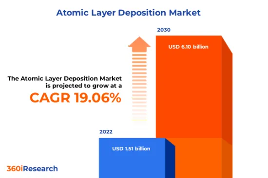
預計2022年原子層沉積市場規模為15.1億美元,2023年預計將達到17.8億美元,2030年將達到61億美元,複合年成長率為19.06%。
原子層沉積的世界市場
| 主要市場統計 | |
|---|---|
| 基準年[2022] | 15.1億美元 |
| 預測年份 [2023] | 17.8億美元 |
| 預測年份 [2030] | 61億美元 |
| 複合年成長率(%) | 19.06% |
原子層沉積是一種用於在基板上高精度沉積薄膜的特殊製程。該技術通常涉及前驅氣體的表面控制沉澱,該前驅氣體在週期性過程中與基板表面發生反應,從而導致原子級沉澱。由於對高性能薄膜、電子產品小型化和可再生能源投資的需求不斷增加,對 ALD 技術的需求正在顯著增加。然而,對於一些公司來說,ALD 設備和材料的初始投資可能金額。此外,ALD 流程的複雜性需要專業知識和培訓,這可能會限制採用。持續的研發活動促進創新並發現 ALD 應用的新途徑。此外,ALD 設備設計和易用性的持續改進有可能提高採用率並降低管理成本。
區域洞察
在美洲,ALD(原子層沉積)的需求主要來自半導體產業,受到電子製造商先進材料需求的推動。該市是領先半導體公司的所在地,專注於創新和高性能塗層解決方案。這些地區的客戶通常優先考慮品質和先進功能而不是成本,這反映在他們的購買行為中。學術和商業機構都在積極進行新材料及其應用的研究。歐盟的特點是強調跨國家和跨產業的合作,以及對永續性的堅定承諾。太陽能發電等應用對 ALD 的需求不斷增加,其中環境因素是首要考慮因素。該地區的客戶普遍具有高度的環保意識,正在尋找兼具性能和環保性的解決方案。 ALD市場以亞太地區為主,以中國、日本和印度為中心。在中國和日本,ALD技術對於電子和汽車產業的發展至關重要,企業正在大力投資研發更好、更具成本效益的ALD解決方案。印度電子製造業的崛起為 ALD 技術帶來了巨大的機會。這些市場的特點是大量生產,成本效率和高品質非常重要。客戶採購往往強調與提供一致且可靠技術的供應商的長期關係。
FPNV定位矩陣
FPNV定位矩陣對於評估原子層沉積市場至關重要。我們檢視與業務策略和產品滿意度相關的關鍵指標,以對供應商進行全面評估。這種深入的分析使用戶能夠根據自己的要求做出明智的決策。根據評估,供應商被分為四個成功程度不同的像限:前沿(F)、探路者(P)、利基(N)和重要(V)。
市場佔有率分析
市場佔有率分析是一種綜合工具,可以對原子層沉積市場供應商的現狀進行深入而深入的研究。全面比較和分析供應商在整體收益、基本客群和其他關鍵指標方面的貢獻,以便更好地了解公司的績效及其在爭奪市場佔有率時面臨的挑戰。此外,該分析還提供了對該行業競爭特徵的寶貴見解,包括在研究基準年觀察到的累積、分散主導地位和合併特徵等因素。這種詳細程度的提高使供應商能夠做出更明智的決策並制定有效的策略,從而在市場上獲得競爭優勢。
該報告對以下幾個方面提供了寶貴的見解:
1-市場滲透率:提供有關主要企業所服務的市場的全面資訊。
2-市場開拓:我們深入研究利潤豐厚的新興市場,並分析它們在成熟細分市場中的滲透率。
3- 市場多元化:提供有關新產品發布、開拓地區、最新發展和投資的詳細資訊。
4-競爭力評估與資訊:對主要企業的市場佔有率、策略、產品、認證、監管狀況、專利狀況、製造能力等進行全面評估。
5- 產品開發與創新:提供對未來技術、研發活動和突破性產品開發的見解。
本報告解決了以下關鍵問題:
1-原子層沉積市場的市場規模與預測是多少?
2-在原子層沉積市場預測期內需要考慮投資的產品、細分市場、應用和領域有哪些?
3-原子層沉積市場的技術趨勢和法律規範是什麼?
4-原子層沉積市場主要供應商的市場佔有率是多少?
5-進入原子層沉積市場的合適型態和策略手段是什麼?
目錄
第1章 前言
第2章調查方法
第3章執行摘要
第4章市場概況
第5章市場洞察
- 市場動態
- 促進因素
- 由於消費性電器產品需求增加,電子和半導體解決方案成長
- 介紹可提高元件小型化以及基板效率和穩定性的材料
- 前端應用的不斷變化以及新一代光電和射頻 (RF) 技術的發展
- 抑制因素
- 研發投入成本高
- 原子層沉積 (ALD) 的替代方案
- 機會
- 政府補貼鼓勵綠色能源來源
- 在醫療植入和穿戴式醫療設備的應用
- 原子層沉積研究和開發的成長
- 任務
- 需要支援多種功能的多功能工具
- 促進因素
- 市場區隔分析
- 類型:由於電氣特性,優選氧化鋁 ALD
- 應用:在半導體工業中有效利用原子層沉積
- 市場趨勢分析
- COVID-19 的累積影響
- 俄羅斯-烏克蘭衝突的累積影響
- 高通膨的累積效應
- 波特五力分析
- 價值鍊和關鍵路徑分析
- 法律規範
- 客戶客製化
第6章原子層沉積市場:依類型
- 氧化鋁 ALD
- 催化劑原子層沉積
- 金屬原子層沉積
- 等離子體增強原子層沉積
第7章原子層沉積市場:依應用
- 電子產品
- 醫療設備
- 半導體
- 太陽能裝置
第8章美洲原子層沉積市場
- 阿根廷
- 巴西
- 加拿大
- 墨西哥
- 美國
第9章亞太地區原子層沉積市場
- 澳洲
- 中國
- 印度
- 印尼
- 日本
- 馬來西亞
- 菲律賓
- 新加坡
- 韓國
- 台灣
- 泰國
- 越南
第10章歐洲、中東和非洲原子層沉積市場
- 丹麥
- 埃及
- 芬蘭
- 法國
- 德國
- 以色列
- 義大利
- 荷蘭
- 奈及利亞
- 挪威
- 波蘭
- 卡達
- 俄羅斯
- 沙烏地阿拉伯
- 南非
- 西班牙
- 瑞典
- 瑞士
- 土耳其
- 阿拉伯聯合大公國
- 英國
第11章競爭形勢
- FPNV定位矩陣
- 市場佔有率分析:主要企業
- 主要企業競爭情境分析
- 合約、合作和夥伴關係
- 新產品發布和功能增強
第12章競爭產品組合
- 主要公司簡介
- Adeka Corporation
- Aixtron SE
- ALD NanoSolutions, Inc.
- Anric Technologies LLC
- Applied Materials Inc.
- Arradiance, LLC
- ASM International NV
- Beneq Oy
- Canon Anvela Corporation
- CVD Equipment Corporation
- Denton Vacuum LLC
- Encapsulix SAS
- Entegris, Inc.
- Eugenus, Inc.
- Forge Nano, Inc.
- Hitachi, Ltd.
- HZO, Inc.
- Kurt J. Lesker Company
- Lam Research Corporation
- Merck KGaA
- NCD Co., Ltd.
- Oxford Instruments PLC
- SENTECH Instruments GmbH
- SkyWater Technology Foundry, Inc.
- Veeco Instruments Inc.
- 主要產品系列
第13章附錄
- 討論指南
- 關於許可證和定價
[190 Pages Report] The Atomic Layer Deposition Market size was estimated at USD 1.51 billion in 2022 and expected to reach USD 1.78 billion in 2023, at a CAGR 19.06% to reach USD 6.10 billion by 2030.
Global Atomic Layer Deposition Market
| KEY MARKET STATISTICS | |
|---|---|
| Base Year [2022] | USD 1.51 billion |
| Estimated Year [2023] | USD 1.78 billion |
| Forecast Year [2030] | USD 6.10 billion |
| CAGR (%) | 19.06% |
Atomic layer deposition is a specialized process used to deposit thin films on substrates with high precision. This technique involves the surface-controlled deposition of precursor gases that react with the surface of a substrate, generally in a cyclic process, leading to atomic-scale deposition. The increasing demand for high-performance films, miniaturization of electronics, and investment in renewable energy have significantly enhanced the demand for ALD technology. However, the initial investment for ALD equipment and materials can be prohibitive for some companies. In addition, the complexity of ALD processes may require specialized knowledge and training, potentially limiting adoption. Furthermore, the ongoing R&D activities drive innovation and uncover new avenues for ALD applications. Moreover, the Continuous improvement in the design and usability of ALD equipment can increase adoption and reduce overhead costs.
Regional Insights
In the Americas, the demand for Atomic Layer Deposition (ALD) largely stems from the semiconductor industry, driven by the advanced material needs of electronics manufacturers. As home to several leading semiconductor firms, the focus has been innovation and high-performance coating solutions. Customers in these regions often prioritize quality and advanced features over cost, which is reflected in their purchasing behaviors. Research into new materials and applications is being actively conducted by both academic and commercial institutions. The EU is characterized by its strong emphasis on collaboration across nations and industries and a keen focus on sustainability. There is a rising demand for ALD in applications such as photovoltaics, where environmental considerations are paramount. Customers here generally have a high degree of environmental awareness and look for solutions that offer both performance and eco-friendliness. The Asia Pacific region, led by China, Japan, and India, is dominant in the ALD market. In China and Japan, ALD technology is integral to the substantial electronics and automotive sectors, with companies heavily investing in R&D for better and more cost-effective ALD solutions. The rising electronics manufacturing industry in India presents a significant opportunity for ALD technologies. These markets are characterized by high-volume manufacturing, where cost-effectiveness and high quality are critical. Customer purchasing tends to emphasize long-term relationships with suppliers who provide consistent and reliable technology.
FPNV Positioning Matrix
The FPNV Positioning Matrix is pivotal in evaluating the Atomic Layer Deposition Market. It offers a comprehensive assessment of vendors, examining key metrics related to Business Strategy and Product Satisfaction. This in-depth analysis empowers users to make well-informed decisions aligned with their requirements. Based on the evaluation, the vendors are then categorized into four distinct quadrants representing varying levels of success: Forefront (F), Pathfinder (P), Niche (N), or Vital (V).
Market Share Analysis
The Market Share Analysis is a comprehensive tool that provides an insightful and in-depth examination of the current state of vendors in the Atomic Layer Deposition Market. By meticulously comparing and analyzing vendor contributions in terms of overall revenue, customer base, and other key metrics, we can offer companies a greater understanding of their performance and the challenges they face when competing for market share. Additionally, this analysis provides valuable insights into the competitive nature of the sector, including factors such as accumulation, fragmentation dominance, and amalgamation traits observed over the base year period studied. With this expanded level of detail, vendors can make more informed decisions and devise effective strategies to gain a competitive edge in the market.
Key Company Profiles
The report delves into recent significant developments in the Atomic Layer Deposition Market, highlighting leading vendors and their innovative profiles. These include Adeka Corporation, Aixtron SE, ALD NanoSolutions, Inc., Anric Technologies LLC, Applied Materials Inc., Arradiance, LLC, ASM International N.V., Beneq Oy, Canon Anvela Corporation, CVD Equipment Corporation, Denton Vacuum LLC, Encapsulix SAS, Entegris, Inc., Eugenus, Inc., Forge Nano, Inc., Hitachi, Ltd., HZO, Inc., Kurt J. Lesker Company, Lam Research Corporation, Merck KGaA, NCD Co., Ltd., Oxford Instruments PLC, SENTECH Instruments GmbH, SkyWater Technology Foundry, Inc., and Veeco Instruments Inc..
Market Segmentation & Coverage
This research report categorizes the Atomic Layer Deposition Market to forecast the revenues and analyze trends in each of the following sub-markets:
- Type
- Aluminum Oxide ALD
- Catalytic ALD
- Metal ALD
- Plasma Enhanced ALD
- Application
- Electronics
- Medical Equipment
- Semiconductors
- Solar Devices
- Region
- Americas
- Argentina
- Brazil
- Canada
- Mexico
- United States
- California
- Florida
- Illinois
- New York
- Ohio
- Pennsylvania
- Texas
- Asia-Pacific
- Australia
- China
- India
- Indonesia
- Japan
- Malaysia
- Philippines
- Singapore
- South Korea
- Taiwan
- Thailand
- Vietnam
- Europe, Middle East & Africa
- Denmark
- Egypt
- Finland
- France
- Germany
- Israel
- Italy
- Netherlands
- Nigeria
- Norway
- Poland
- Qatar
- Russia
- Saudi Arabia
- South Africa
- Spain
- Sweden
- Switzerland
- Turkey
- United Arab Emirates
- United Kingdom
- Americas
The report offers valuable insights on the following aspects:
1. Market Penetration: It presents comprehensive information on the market provided by key players.
2. Market Development: It delves deep into lucrative emerging markets and analyzes the penetration across mature market segments.
3. Market Diversification: It provides detailed information on new product launches, untapped geographic regions, recent developments, and investments.
4. Competitive Assessment & Intelligence: It conducts an exhaustive assessment of market shares, strategies, products, certifications, regulatory approvals, patent landscape, and manufacturing capabilities of the leading players.
5. Product Development & Innovation: It offers intelligent insights on future technologies, R&D activities, and breakthrough product developments.
The report addresses key questions such as:
1. What is the market size and forecast of the Atomic Layer Deposition Market?
2. Which products, segments, applications, and areas should one consider investing in over the forecast period in the Atomic Layer Deposition Market?
3. What are the technology trends and regulatory frameworks in the Atomic Layer Deposition Market?
4. What is the market share of the leading vendors in the Atomic Layer Deposition Market?
5. Which modes and strategic moves are suitable for entering the Atomic Layer Deposition Market?
Table of Contents
1. Preface
- 1.1. Objectives of the Study
- 1.2. Market Segmentation & Coverage
- 1.3. Years Considered for the Study
- 1.4. Currency & Pricing
- 1.5. Language
- 1.6. Limitations
- 1.7. Assumptions
- 1.8. Stakeholders
2. Research Methodology
- 2.1. Define: Research Objective
- 2.2. Determine: Research Design
- 2.3. Prepare: Research Instrument
- 2.4. Collect: Data Source
- 2.5. Analyze: Data Interpretation
- 2.6. Formulate: Data Verification
- 2.7. Publish: Research Report
- 2.8. Repeat: Report Update
3. Executive Summary
4. Market Overview
- 4.1. Introduction
- 4.2. Atomic Layer Deposition Market, by Region
5. Market Insights
- 5.1. Market Dynamics
- 5.1.1. Drivers
- 5.1.1.1. Growing electronics and semiconductor solutions accompanied by increase in the demand of consumer electronics
- 5.1.1.2. Component miniaturization and introduction of materials offering higher efficiency and stability of substrates
- 5.1.1.3. Increasing inflections in front end applications and evolution of a new gneneration of photonics and radio frequency (RF) technologies
- 5.1.2. Restraints
- 5.1.2.1. High investment Cost in R&D
- 5.1.2.2. Alternatives of Atomic Layer Deposition (ALD)
- 5.1.3. Opportunities
- 5.1.3.1. Subsidies offered by government encouraging green energy sources
- 5.1.3.2. Applications in medical implants and wearable medical devices
- 5.1.3.3. Growing R&D in atomic layer deposition
- 5.1.4. Challenges
- 5.1.4.1. Need for versatile tools to support multiple capabilities
- 5.1.1. Drivers
- 5.2. Market Segmentation Analysis
- 5.2.1. Type: Preference towards Aluminum Oxide ALD due to its electrical properties
- 5.2.2. Application: Significant utilization of atomic layer deposition in semiconductor industry
- 5.3. Market Trend Analysis
- 5.4. Cumulative Impact of COVID-19
- 5.5. Cumulative Impact of Russia-Ukraine Conflict
- 5.6. Cumulative Impact of High Inflation
- 5.7. Porter's Five Forces Analysis
- 5.7.1. Threat of New Entrants
- 5.7.2. Threat of Substitutes
- 5.7.3. Bargaining Power of Customers
- 5.7.4. Bargaining Power of Suppliers
- 5.7.5. Industry Rivalry
- 5.8. Value Chain & Critical Path Analysis
- 5.9. Regulatory Framework
- 5.10. Client Customization
6. Atomic Layer Deposition Market, by Type
- 6.1. Introduction
- 6.2. Aluminum Oxide ALD
- 6.3. Catalytic ALD
- 6.4. Metal ALD
- 6.5. Plasma Enhanced ALD
7. Atomic Layer Deposition Market, by Application
- 7.1. Introduction
- 7.2. Electronics
- 7.3. Medical Equipment
- 7.4. Semiconductors
- 7.5. Solar Devices
8. Americas Atomic Layer Deposition Market
- 8.1. Introduction
- 8.2. Argentina
- 8.3. Brazil
- 8.4. Canada
- 8.5. Mexico
- 8.6. United States
9. Asia-Pacific Atomic Layer Deposition Market
- 9.1. Introduction
- 9.2. Australia
- 9.3. China
- 9.4. India
- 9.5. Indonesia
- 9.6. Japan
- 9.7. Malaysia
- 9.8. Philippines
- 9.9. Singapore
- 9.10. South Korea
- 9.11. Taiwan
- 9.12. Thailand
- 9.13. Vietnam
10. Europe, Middle East & Africa Atomic Layer Deposition Market
- 10.1. Introduction
- 10.2. Denmark
- 10.3. Egypt
- 10.4. Finland
- 10.5. France
- 10.6. Germany
- 10.7. Israel
- 10.8. Italy
- 10.9. Netherlands
- 10.10. Nigeria
- 10.11. Norway
- 10.12. Poland
- 10.13. Qatar
- 10.14. Russia
- 10.15. Saudi Arabia
- 10.16. South Africa
- 10.17. Spain
- 10.18. Sweden
- 10.19. Switzerland
- 10.20. Turkey
- 10.21. United Arab Emirates
- 10.22. United Kingdom
11. Competitive Landscape
- 11.1. FPNV Positioning Matrix
- 11.2. Market Share Analysis, By Key Player
- 11.3. Competitive Scenario Analysis, By Key Player
- 11.3.1. Agreement, Collaboration, & Partnership
- 11.3.1.1. 6K Energy to Implement Forge Nano Equipment for Commercial Production of NMC 811
- 11.3.2. New Product Launch & Enhancement
- 11.3.2.1. SkyWater Installs an Atomic Layer Deposition System for the Development and Production of Advanced Technologies
- 11.3.2.2. Oxford Instruments Launches Breakthrough Ultra-fast ALD Product for Quantum Technology and Advanced R&D
- 11.3.1. Agreement, Collaboration, & Partnership
12. Competitive Portfolio
- 12.1. Key Company Profiles
- 12.1.1. Adeka Corporation
- 12.1.2. Aixtron SE
- 12.1.3. ALD NanoSolutions, Inc.
- 12.1.4. Anric Technologies LLC
- 12.1.5. Applied Materials Inc.
- 12.1.6. Arradiance, LLC
- 12.1.7. ASM International N.V.
- 12.1.8. Beneq Oy
- 12.1.9. Canon Anvela Corporation
- 12.1.10. CVD Equipment Corporation
- 12.1.11. Denton Vacuum LLC
- 12.1.12. Encapsulix SAS
- 12.1.13. Entegris, Inc.
- 12.1.14. Eugenus, Inc.
- 12.1.15. Forge Nano, Inc.
- 12.1.16. Hitachi, Ltd.
- 12.1.17. HZO, Inc.
- 12.1.18. Kurt J. Lesker Company
- 12.1.19. Lam Research Corporation
- 12.1.20. Merck KGaA
- 12.1.21. NCD Co., Ltd.
- 12.1.22. Oxford Instruments PLC
- 12.1.23. SENTECH Instruments GmbH
- 12.1.24. SkyWater Technology Foundry, Inc.
- 12.1.25. Veeco Instruments Inc.
- 12.2. Key Product Portfolio
13. Appendix
- 13.1. Discussion Guide
- 13.2. License & Pricing
LIST OF FIGURES
- FIGURE 1. ATOMIC LAYER DEPOSITION MARKET RESEARCH PROCESS
- FIGURE 2. ATOMIC LAYER DEPOSITION MARKET SIZE, 2022 VS 2030
- FIGURE 3. ATOMIC LAYER DEPOSITION MARKET SIZE, 2018-2030 (USD MILLION)
- FIGURE 4. ATOMIC LAYER DEPOSITION MARKET SIZE, BY REGION, 2022 VS 2030 (%)
- FIGURE 5. ATOMIC LAYER DEPOSITION MARKET SIZE, BY REGION, 2022 VS 2023 VS 2030 (USD MILLION)
- FIGURE 6. ATOMIC LAYER DEPOSITION MARKET DYNAMICS
- FIGURE 7. ATOMIC LAYER DEPOSITION MARKET SIZE, BY TYPE, 2022 VS 2030 (%)
- FIGURE 8. ATOMIC LAYER DEPOSITION MARKET SIZE, BY TYPE, 2022 VS 2023 VS 2030 (USD MILLION)
- FIGURE 9. ATOMIC LAYER DEPOSITION MARKET SIZE, BY APPLICATION, 2022 VS 2030 (%)
- FIGURE 10. ATOMIC LAYER DEPOSITION MARKET SIZE, BY APPLICATION, 2022 VS 2023 VS 2030 (USD MILLION)
- FIGURE 11. AMERICAS ATOMIC LAYER DEPOSITION MARKET SIZE, BY COUNTRY, 2022 VS 2030 (%)
- FIGURE 12. AMERICAS ATOMIC LAYER DEPOSITION MARKET SIZE, BY COUNTRY, 2022 VS 2023 VS 2030 (USD MILLION)
- FIGURE 13. UNITED STATES ATOMIC LAYER DEPOSITION MARKET SIZE, BY STATE, 2022 VS 2030 (%)
- FIGURE 14. UNITED STATES ATOMIC LAYER DEPOSITION MARKET SIZE, BY STATE, 2022 VS 2023 VS 2030 (USD MILLION)
- FIGURE 15. ASIA-PACIFIC ATOMIC LAYER DEPOSITION MARKET SIZE, BY COUNTRY, 2022 VS 2030 (%)
- FIGURE 16. ASIA-PACIFIC ATOMIC LAYER DEPOSITION MARKET SIZE, BY COUNTRY, 2022 VS 2023 VS 2030 (USD MILLION)
- FIGURE 17. EUROPE, MIDDLE EAST & AFRICA ATOMIC LAYER DEPOSITION MARKET SIZE, BY COUNTRY, 2022 VS 2030 (%)
- FIGURE 18. EUROPE, MIDDLE EAST & AFRICA ATOMIC LAYER DEPOSITION MARKET SIZE, BY COUNTRY, 2022 VS 2023 VS 2030 (USD MILLION)
- FIGURE 19. ATOMIC LAYER DEPOSITION MARKET, FPNV POSITIONING MATRIX, 2022
- FIGURE 20. ATOMIC LAYER DEPOSITION MARKET SHARE, BY KEY PLAYER, 2022
LIST OF TABLES
- TABLE 1. ATOMIC LAYER DEPOSITION MARKET SEGMENTATION & COVERAGE
- TABLE 2. UNITED STATES DOLLAR EXCHANGE RATE, 2018-2022
- TABLE 3. ATOMIC LAYER DEPOSITION MARKET SIZE, 2018-2030 (USD MILLION)
- TABLE 4. GLOBAL ATOMIC LAYER DEPOSITION MARKET SIZE, BY REGION, 2018-2030 (USD MILLION)
- TABLE 5. ATOMIC LAYER DEPOSITION MARKET SIZE, BY TYPE, 2018-2030 (USD MILLION)
- TABLE 6. ATOMIC LAYER DEPOSITION MARKET SIZE, BY ALUMINUM OXIDE ALD, BY REGION, 2018-2030 (USD MILLION)
- TABLE 7. ATOMIC LAYER DEPOSITION MARKET SIZE, BY CATALYTIC ALD, BY REGION, 2018-2030 (USD MILLION)
- TABLE 8. ATOMIC LAYER DEPOSITION MARKET SIZE, BY METAL ALD, BY REGION, 2018-2030 (USD MILLION)
- TABLE 9. ATOMIC LAYER DEPOSITION MARKET SIZE, BY PLASMA ENHANCED ALD, BY REGION, 2018-2030 (USD MILLION)
- TABLE 10. ATOMIC LAYER DEPOSITION MARKET SIZE, BY APPLICATION, 2018-2030 (USD MILLION)
- TABLE 11. ATOMIC LAYER DEPOSITION MARKET SIZE, BY ELECTRONICS, BY REGION, 2018-2030 (USD MILLION)
- TABLE 12. ATOMIC LAYER DEPOSITION MARKET SIZE, BY MEDICAL EQUIPMENT, BY REGION, 2018-2030 (USD MILLION)
- TABLE 13. ATOMIC LAYER DEPOSITION MARKET SIZE, BY SEMICONDUCTORS, BY REGION, 2018-2030 (USD MILLION)
- TABLE 14. ATOMIC LAYER DEPOSITION MARKET SIZE, BY SOLAR DEVICES, BY REGION, 2018-2030 (USD MILLION)
- TABLE 15. AMERICAS ATOMIC LAYER DEPOSITION MARKET SIZE, BY TYPE, 2018-2030 (USD MILLION)
- TABLE 16. AMERICAS ATOMIC LAYER DEPOSITION MARKET SIZE, BY APPLICATION, 2018-2030 (USD MILLION)
- TABLE 17. AMERICAS ATOMIC LAYER DEPOSITION MARKET SIZE, BY COUNTRY, 2018-2030 (USD MILLION)
- TABLE 18. ARGENTINA ATOMIC LAYER DEPOSITION MARKET SIZE, BY TYPE, 2018-2030 (USD MILLION)
- TABLE 19. ARGENTINA ATOMIC LAYER DEPOSITION MARKET SIZE, BY APPLICATION, 2018-2030 (USD MILLION)
- TABLE 20. BRAZIL ATOMIC LAYER DEPOSITION MARKET SIZE, BY TYPE, 2018-2030 (USD MILLION)
- TABLE 21. BRAZIL ATOMIC LAYER DEPOSITION MARKET SIZE, BY APPLICATION, 2018-2030 (USD MILLION)
- TABLE 22. CANADA ATOMIC LAYER DEPOSITION MARKET SIZE, BY TYPE, 2018-2030 (USD MILLION)
- TABLE 23. CANADA ATOMIC LAYER DEPOSITION MARKET SIZE, BY APPLICATION, 2018-2030 (USD MILLION)
- TABLE 24. MEXICO ATOMIC LAYER DEPOSITION MARKET SIZE, BY TYPE, 2018-2030 (USD MILLION)
- TABLE 25. MEXICO ATOMIC LAYER DEPOSITION MARKET SIZE, BY APPLICATION, 2018-2030 (USD MILLION)
- TABLE 26. UNITED STATES ATOMIC LAYER DEPOSITION MARKET SIZE, BY TYPE, 2018-2030 (USD MILLION)
- TABLE 27. UNITED STATES ATOMIC LAYER DEPOSITION MARKET SIZE, BY APPLICATION, 2018-2030 (USD MILLION)
- TABLE 28. UNITED STATES ATOMIC LAYER DEPOSITION MARKET SIZE, BY STATE, 2018-2030 (USD MILLION)
- TABLE 29. ASIA-PACIFIC ATOMIC LAYER DEPOSITION MARKET SIZE, BY TYPE, 2018-2030 (USD MILLION)
- TABLE 30. ASIA-PACIFIC ATOMIC LAYER DEPOSITION MARKET SIZE, BY APPLICATION, 2018-2030 (USD MILLION)
- TABLE 31. ASIA-PACIFIC ATOMIC LAYER DEPOSITION MARKET SIZE, BY COUNTRY, 2018-2030 (USD MILLION)
- TABLE 32. AUSTRALIA ATOMIC LAYER DEPOSITION MARKET SIZE, BY TYPE, 2018-2030 (USD MILLION)
- TABLE 33. AUSTRALIA ATOMIC LAYER DEPOSITION MARKET SIZE, BY APPLICATION, 2018-2030 (USD MILLION)
- TABLE 34. CHINA ATOMIC LAYER DEPOSITION MARKET SIZE, BY TYPE, 2018-2030 (USD MILLION)
- TABLE 35. CHINA ATOMIC LAYER DEPOSITION MARKET SIZE, BY APPLICATION, 2018-2030 (USD MILLION)
- TABLE 36. INDIA ATOMIC LAYER DEPOSITION MARKET SIZE, BY TYPE, 2018-2030 (USD MILLION)
- TABLE 37. INDIA ATOMIC LAYER DEPOSITION MARKET SIZE, BY APPLICATION, 2018-2030 (USD MILLION)
- TABLE 38. INDONESIA ATOMIC LAYER DEPOSITION MARKET SIZE, BY TYPE, 2018-2030 (USD MILLION)
- TABLE 39. INDONESIA ATOMIC LAYER DEPOSITION MARKET SIZE, BY APPLICATION, 2018-2030 (USD MILLION)
- TABLE 40. JAPAN ATOMIC LAYER DEPOSITION MARKET SIZE, BY TYPE, 2018-2030 (USD MILLION)
- TABLE 41. JAPAN ATOMIC LAYER DEPOSITION MARKET SIZE, BY APPLICATION, 2018-2030 (USD MILLION)
- TABLE 42. MALAYSIA ATOMIC LAYER DEPOSITION MARKET SIZE, BY TYPE, 2018-2030 (USD MILLION)
- TABLE 43. MALAYSIA ATOMIC LAYER DEPOSITION MARKET SIZE, BY APPLICATION, 2018-2030 (USD MILLION)
- TABLE 44. PHILIPPINES ATOMIC LAYER DEPOSITION MARKET SIZE, BY TYPE, 2018-2030 (USD MILLION)
- TABLE 45. PHILIPPINES ATOMIC LAYER DEPOSITION MARKET SIZE, BY APPLICATION, 2018-2030 (USD MILLION)
- TABLE 46. SINGAPORE ATOMIC LAYER DEPOSITION MARKET SIZE, BY TYPE, 2018-2030 (USD MILLION)
- TABLE 47. SINGAPORE ATOMIC LAYER DEPOSITION MARKET SIZE, BY APPLICATION, 2018-2030 (USD MILLION)
- TABLE 48. SOUTH KOREA ATOMIC LAYER DEPOSITION MARKET SIZE, BY TYPE, 2018-2030 (USD MILLION)
- TABLE 49. SOUTH KOREA ATOMIC LAYER DEPOSITION MARKET SIZE, BY APPLICATION, 2018-2030 (USD MILLION)
- TABLE 50. TAIWAN ATOMIC LAYER DEPOSITION MARKET SIZE, BY TYPE, 2018-2030 (USD MILLION)
- TABLE 51. TAIWAN ATOMIC LAYER DEPOSITION MARKET SIZE, BY APPLICATION, 2018-2030 (USD MILLION)
- TABLE 52. THAILAND ATOMIC LAYER DEPOSITION MARKET SIZE, BY TYPE, 2018-2030 (USD MILLION)
- TABLE 53. THAILAND ATOMIC LAYER DEPOSITION MARKET SIZE, BY APPLICATION, 2018-2030 (USD MILLION)
- TABLE 54. VIETNAM ATOMIC LAYER DEPOSITION MARKET SIZE, BY TYPE, 2018-2030 (USD MILLION)
- TABLE 55. VIETNAM ATOMIC LAYER DEPOSITION MARKET SIZE, BY APPLICATION, 2018-2030 (USD MILLION)
- TABLE 56. EUROPE, MIDDLE EAST & AFRICA ATOMIC LAYER DEPOSITION MARKET SIZE, BY TYPE, 2018-2030 (USD MILLION)
- TABLE 57. EUROPE, MIDDLE EAST & AFRICA ATOMIC LAYER DEPOSITION MARKET SIZE, BY APPLICATION, 2018-2030 (USD MILLION)
- TABLE 58. EUROPE, MIDDLE EAST & AFRICA ATOMIC LAYER DEPOSITION MARKET SIZE, BY COUNTRY, 2018-2030 (USD MILLION)
- TABLE 59. DENMARK ATOMIC LAYER DEPOSITION MARKET SIZE, BY TYPE, 2018-2030 (USD MILLION)
- TABLE 60. DENMARK ATOMIC LAYER DEPOSITION MARKET SIZE, BY APPLICATION, 2018-2030 (USD MILLION)
- TABLE 61. EGYPT ATOMIC LAYER DEPOSITION MARKET SIZE, BY TYPE, 2018-2030 (USD MILLION)
- TABLE 62. EGYPT ATOMIC LAYER DEPOSITION MARKET SIZE, BY APPLICATION, 2018-2030 (USD MILLION)
- TABLE 63. FINLAND ATOMIC LAYER DEPOSITION MARKET SIZE, BY TYPE, 2018-2030 (USD MILLION)
- TABLE 64. FINLAND ATOMIC LAYER DEPOSITION MARKET SIZE, BY APPLICATION, 2018-2030 (USD MILLION)
- TABLE 65. FRANCE ATOMIC LAYER DEPOSITION MARKET SIZE, BY TYPE, 2018-2030 (USD MILLION)
- TABLE 66. FRANCE ATOMIC LAYER DEPOSITION MARKET SIZE, BY APPLICATION, 2018-2030 (USD MILLION)
- TABLE 67. GERMANY ATOMIC LAYER DEPOSITION MARKET SIZE, BY TYPE, 2018-2030 (USD MILLION)
- TABLE 68. GERMANY ATOMIC LAYER DEPOSITION MARKET SIZE, BY APPLICATION, 2018-2030 (USD MILLION)
- TABLE 69. ISRAEL ATOMIC LAYER DEPOSITION MARKET SIZE, BY TYPE, 2018-2030 (USD MILLION)
- TABLE 70. ISRAEL ATOMIC LAYER DEPOSITION MARKET SIZE, BY APPLICATION, 2018-2030 (USD MILLION)
- TABLE 71. ITALY ATOMIC LAYER DEPOSITION MARKET SIZE, BY TYPE, 2018-2030 (USD MILLION)
- TABLE 72. ITALY ATOMIC LAYER DEPOSITION MARKET SIZE, BY APPLICATION, 2018-2030 (USD MILLION)
- TABLE 73. NETHERLANDS ATOMIC LAYER DEPOSITION MARKET SIZE, BY TYPE, 2018-2030 (USD MILLION)
- TABLE 74. NETHERLANDS ATOMIC LAYER DEPOSITION MARKET SIZE, BY APPLICATION, 2018-2030 (USD MILLION)
- TABLE 75. NIGERIA ATOMIC LAYER DEPOSITION MARKET SIZE, BY TYPE, 2018-2030 (USD MILLION)
- TABLE 76. NIGERIA ATOMIC LAYER DEPOSITION MARKET SIZE, BY APPLICATION, 2018-2030 (USD MILLION)
- TABLE 77. NORWAY ATOMIC LAYER DEPOSITION MARKET SIZE, BY TYPE, 2018-2030 (USD MILLION)
- TABLE 78. NORWAY ATOMIC LAYER DEPOSITION MARKET SIZE, BY APPLICATION, 2018-2030 (USD MILLION)
- TABLE 79. POLAND ATOMIC LAYER DEPOSITION MARKET SIZE, BY TYPE, 2018-2030 (USD MILLION)
- TABLE 80. POLAND ATOMIC LAYER DEPOSITION MARKET SIZE, BY APPLICATION, 2018-2030 (USD MILLION)
- TABLE 81. QATAR ATOMIC LAYER DEPOSITION MARKET SIZE, BY TYPE, 2018-2030 (USD MILLION)
- TABLE 82. QATAR ATOMIC LAYER DEPOSITION MARKET SIZE, BY APPLICATION, 2018-2030 (USD MILLION)
- TABLE 83. RUSSIA ATOMIC LAYER DEPOSITION MARKET SIZE, BY TYPE, 2018-2030 (USD MILLION)
- TABLE 84. RUSSIA ATOMIC LAYER DEPOSITION MARKET SIZE, BY APPLICATION, 2018-2030 (USD MILLION)
- TABLE 85. SAUDI ARABIA ATOMIC LAYER DEPOSITION MARKET SIZE, BY TYPE, 2018-2030 (USD MILLION)
- TABLE 86. SAUDI ARABIA ATOMIC LAYER DEPOSITION MARKET SIZE, BY APPLICATION, 2018-2030 (USD MILLION)
- TABLE 87. SOUTH AFRICA ATOMIC LAYER DEPOSITION MARKET SIZE, BY TYPE, 2018-2030 (USD MILLION)
- TABLE 88. SOUTH AFRICA ATOMIC LAYER DEPOSITION MARKET SIZE, BY APPLICATION, 2018-2030 (USD MILLION)
- TABLE 89. SPAIN ATOMIC LAYER DEPOSITION MARKET SIZE, BY TYPE, 2018-2030 (USD MILLION)
- TABLE 90. SPAIN ATOMIC LAYER DEPOSITION MARKET SIZE, BY APPLICATION, 2018-2030 (USD MILLION)
- TABLE 91. SWEDEN ATOMIC LAYER DEPOSITION MARKET SIZE, BY TYPE, 2018-2030 (USD MILLION)
- TABLE 92. SWEDEN ATOMIC LAYER DEPOSITION MARKET SIZE, BY APPLICATION, 2018-2030 (USD MILLION)
- TABLE 93. SWITZERLAND ATOMIC LAYER DEPOSITION MARKET SIZE, BY TYPE, 2018-2030 (USD MILLION)
- TABLE 94. SWITZERLAND ATOMIC LAYER DEPOSITION MARKET SIZE, BY APPLICATION, 2018-2030 (USD MILLION)
- TABLE 95. TURKEY ATOMIC LAYER DEPOSITION MARKET SIZE, BY TYPE, 2018-2030 (USD MILLION)
- TABLE 96. TURKEY ATOMIC LAYER DEPOSITION MARKET SIZE, BY APPLICATION, 2018-2030 (USD MILLION)
- TABLE 97. UNITED ARAB EMIRATES ATOMIC LAYER DEPOSITION MARKET SIZE, BY TYPE, 2018-2030 (USD MILLION)
- TABLE 98. UNITED ARAB EMIRATES ATOMIC LAYER DEPOSITION MARKET SIZE, BY APPLICATION, 2018-2030 (USD MILLION)
- TABLE 99. UNITED KINGDOM ATOMIC LAYER DEPOSITION MARKET SIZE, BY TYPE, 2018-2030 (USD MILLION)
- TABLE 100. UNITED KINGDOM ATOMIC LAYER DEPOSITION MARKET SIZE, BY APPLICATION, 2018-2030 (USD MILLION)
- TABLE 101. ATOMIC LAYER DEPOSITION MARKET, FPNV POSITIONING MATRIX, 2022
- TABLE 102. ATOMIC LAYER DEPOSITION MARKET SHARE, BY KEY PLAYER, 2022
- TABLE 103. ATOMIC LAYER DEPOSITION MARKET LICENSE & PRICING
 原子層沉澱設備市場:按沉積方法、薄膜類型和應用分類 - 2024-2030 年全球預測
 原子層沉積設備市場報告(按產品(金屬 ALD、氧化鋁 ALD、等離子體增強 ALD、催化 ALD 等)、應用(半導體、太陽能設備、電子、醫療設備等)和地區 2024-2032
 ALD 設備市場 - 按設備、按沉積方法、按薄膜類型、按應用和預測,2024 年 - 2032 年
 ALD 設備世界市場報告 2024
 半導體市場報告的 ALD 和 CVD 前驅物:2030 年趨勢、預測和競爭分析
 ALD(原子層沉積)2024 年全球市場報告
 原子層沉積設備:市場佔有率分析、產業趨勢與統計、2024年至2029年成長預測
 全球 ALD 設備市場研究報告 - 2023 年至 2030 年產業分析、規模、佔有率、成長、趨勢和預測
 ALD 設備的全球市場:按沉積方法、薄膜類型、半導體應用、非半導體應用、地區 - 預測(截至 2028 年)
 原子層沉積市場:依產品、依用途、依地區