


 |
市場調查報告書
商品編碼
1433512
薄晶圓加工和切割設備的全球市場:市場佔有率分析、行業趨勢/統計、成長預測(2024-2029)Thin Wafer Processing and Dicing Equipment - Market Share Analysis, Industry Trends & Statistics, Growth Forecasts (2024 - 2029) |
||||||
※ 本網頁內容可能與最新版本有所差異。詳細情況請與我們聯繫。
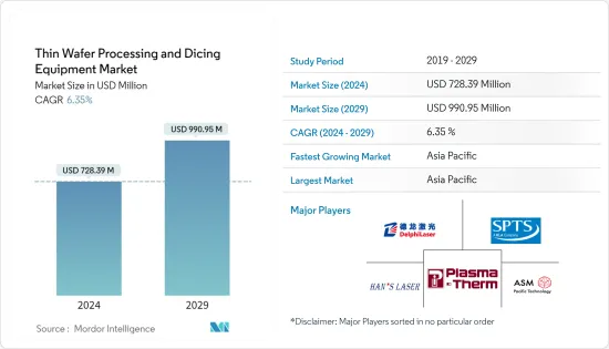
預計2024年全球薄晶圓加工和切割設備市場規模為7.2839億美元,2029年將達到9.9095億美元,在預測期內(2024-2029年)年複合成長率為6,預計將成長35 %。
由於使用量的增加,對電子元件的巨大需求促使人們加強努力,使電子封裝具有高度的資源效率,使其可用於多種應用。這些因素正在推動半導體和IC封裝市場的成長。
主要亮點
- 預計未來幾年推動薄晶圓加工和切割設備需求的主要因素之一是其在記憶卡、智慧型手機、智慧卡和各種運算3D電路。 3D電路被用於多種空間受限的應用,如行動家電、感測器、MEMS和工業產品,因為它們提高了整體產品性能,包括高速、耐用、低功耗和輕量化記憶體,越來越普及。
- 隨著低成本雲端運算解決方案的普及增加了各種企業和產業對伺服器和資料中心系統的使用,對微處理器和數位訊號處理器邏輯裝置設備的普及可能會增加。此外,隨著支援物聯網的連結設備的增加,微處理器的利用率也在增加。這些設備擴大採用薄晶圓來實現有效的熱管理並提高性能。所有這些原因都在推動邏輯裝置市場的擴張。
- 多年來,矽晶圓一直被用作微電子和 MEMS 的製造平台。絕緣體上矽基基板是標準矽晶圓的獨特變體。為了製造這種晶圓,需要使用大約 1 至 2 公尺厚的二氧化矽黏合層將兩個矽晶圓黏合在一起。單片晶圓被壓平至10至50公尺的厚度。塗層的確切厚度取決於應用。
- 建造最先進的薄晶圓代工廠的成本呈指數級上升,對產業帶來壓力。半導體製造商現在已經集中。隨著性能提昇放緩,特種薄晶圓變得越來越有吸引力。使薄晶圓無所不在的設計決策對於某些運算任務來說可能不是最佳的。
- 由於全球工業和汽車電子產品的需求放緩,並因 COVID-19 大流行而加劇,該市場的企業發展商的薄晶圓半導體訂單有所下降。
薄晶圓加工切割設備市場趨勢
對半導體小型化的需求不斷成長正在推動市場發展
- 家用電器、醫療保健和汽車等領域對小型電子設備的需求不斷成長,迫使半導體 IC 製造商縮小其 IC 尺寸。因此,預計在預測期內市場將縮小,需求將激增。
- 從地區來看,無晶圓廠經營模式是亞洲國家在全球半導體銷售中佔據突出地位的關鍵因素。無廠半導體公司通常將製造業務委託給晶圓代工廠、組裝和測試 (OSAT) 公司。根據半導體產業協會(SIA)發布的報告,2021年美國的主導地位自1990年以來顯著下降,僅佔半導體製造能力的12%。東亞特別是中國的崛起得益於各國政府提供的各種獎勵和補貼。
- FUJIFILM表示,由於人工智慧、物聯網、下一代通訊標準5G的廣泛使用以及自動駕駛技術的進步,預計半導體的需求將進一步增加,性能將得到改善,因此半導體裝置的小型化仍在繼續。由於上述因素,對小型輕量消費設備的需求不斷成長,這些設備依賴於超薄矽晶圓上構建的3D電路架構,並有望提供峰值性能。
- 該晶圓非常薄且平坦。同時,小型化產生了在單一晶片上整合多種功能的需求。晶圓尺寸的不斷增大(直徑高達 12 吋)正在推動晶圓技術的新趨勢。
- 2021 年 5 月,IBM 宣佈在半導體設計和加工方面取得突破,發明了首款採用 2 奈米 (nm) 奈米片技術的晶片。半導體應用廣泛,包括電腦、消費性電子產品、通訊設備、運輸系統和關鍵基礎設施。尤其是在混合雲端、AI、物聯網時代,對晶片效能和能源效率有著強烈的需求。 IBM 創新的 2nm 晶片技術推進了半導體產業的最尖端科技,以滿足這種不斷成長的需求。 IBM 的 2nm 晶片技術預計將比目前最先進的 7nm 晶片提供 45% 的性能提升和 75% 的能耗降低。
亞太地區佔最大市場佔有率佔有率
- 亞太地區是全球最大且成長最快的半導體市場。中國、韓國和新加坡等國家對智慧型手機和其他消費性電子產品的龐大需求鼓勵許多供應商在該地區設立生產基地。
- 該市場上的眾多中國企業正致力於透過收購和合併來擴大業務。例如,2021年8月,WaferTech透過其荷蘭子公司Nexperia以約6,300萬歐元收購了Newport Wafer Fab。根據聞泰向上海證券交易所提交的聲明,此次收購於 7 月宣布,並確認了交易條款。聞泰科技是一家組裝智慧型手機和其他家用電器的上市製造商。
- 日本擁有多家主要製造商和電子產業,在半導體產業中佔有不可或缺的地位。預計政府將啟動一項研究,評估主要晶片製造商向該國擴張的可能性。同時,總部位於日本的組織被認為是半導體製造和封裝中消耗的大多數關鍵材料的主要供應商。對於日本供應商來說,日本的外匯和高生產成本使得材料更加昂貴,並為其他低階應用供應商提供了商機。
- 在澳大利亞,電子製造業的成長以及各種最終用途行業擴大採用先進設備正在影響市場的成長。電視和智慧型手機的銷售主要推動家用電器的成長。
- 2021年10月,Quad Alliance還在澳洲、印度、美國和日本發起了半導體供應鏈舉措,旨在繪製半導體及其關鍵零件的產能分佈圖、識別漏洞並加強供應鏈安全。與新南威爾斯州半導體產業服務管理局一起,這些是將澳洲打造為亞太地區參與者並確保我們在全球半導體供應鏈中的地位的正確步驟。
- 目前,印度的半導體需求主要透過進口來滿足。因此,需要對獎勵鏈進行激勵,使印度在經濟上自力更生,在技術上處於領先地位。 2021 年 12 月,政府設想實施一項預算超過 7,600 萬印度盧比的綜合計劃,以發展印度的半導體和顯示器製造生態系統。新計畫下的財政支持力道達2.3億印度盧比,涵蓋電氣設備等整個供應鏈。
- 全自動駕駛汽車的成長軌跡將取決於亞太地區的因素,包括技術進步、消費者接受全自動駕駛汽車的意願、定價以及供應商和OEM解決關鍵車輛安全問題的能力,這些都將受到很大影響。由於這些因素,汽車和半導體產業不斷致力於增強技術、協商原料價格,並最終將汽車與可靠的技術結合。
薄晶圓加工及切割設備產業概況
薄晶圓加工和切割設備市場僅由少數幾家主要公司組成,包括DISCO、Panasonic、日本和台灣脈衝馬達。此外,市場在薄晶圓製造流程方面仍面臨重大挑戰。上述因素也導致新參與企業進入市場的延遲。然而,市場參與者不斷的創新和研發努力保持了競爭力。因此,估計當前市場上競爭公司之間的敵意是溫和的。
- 2022 年 4 月 - DISCO 公司宣布獲得英特爾 EPIC 傑出供應商獎。該獎項旨在表彰在所有績效標準上始終如一的高水準績效。
- 2022年1月-總部位於東京的橫河電機公司與沙烏地阿美公司簽署了一份合作備忘錄,探討在沙烏地阿拉伯王國實現半導體晶片製造在地化的可能性。
其他福利:
- Excel 格式的市場預測 (ME) 表
- 3 個月分析師支持
目錄
第1章簡介
- 研究假設和市場定義
- 調查範圍
第2章調查方法
第3章執行摘要
第4章市場洞察
- 市場概況
- 市場促進與市場約束因素介紹
- 產業吸引力:波特五力分析
- 新進入者的威脅
- 買方議價能力
- 供應商的議價能力
- 替代品的威脅
- 競爭公司之間敵對關係的強度
- 產業價值鏈分析
- COVID-19 市場影響評估
第5章市場動態
- 市場促進因素
- 對智慧卡、RFID 技術和汽車電源 IC 的需求增加
- 對半導體小型化的需求日益成長
- 市場限制因素
- 製造挑戰
第6章市場區隔
- 依設備類型
- 細化裝置
- 刮片設備
- 刀片切割
- 雷射消熔
- 隱形切割
- 等離子切割
- 按用途
- 記憶體邏輯 (TSV)
- 微機電系統元件
- 功率元件
- CMOS影像感測器
- RFID
- 晶圓厚度趨勢
- 按晶圓尺寸
- 小於4英寸
- 5寸和6寸
- 8吋
- 12寸
- 按地區
- 北美洲
- 美國
- 加拿大
- 歐洲
- 英國
- 德國
- 法國
- 西班牙
- 義大利
- 其他歐洲國家
- 亞太地區
- 中國
- 日本
- 澳洲
- 印度
- 其他亞太地區
- 拉丁美洲
- 墨西哥
- 巴西
- 其他拉丁美洲
- 中東/非洲
- 南非
- 沙烏地阿拉伯
- 其他中東/非洲
- 北美洲
第7章 競爭形勢
- 公司簡介
- Suzhou Delphi Laser Co. Ltd
- SPTS Technologies Limited
- Plasma-Therm LLC
- Han's Laser Technology Industry Group Co. Ltd
- ASM Laser Separation International(ALSI)BV
- Disco Corporation
- Tokyo Seimitsu Co, Ltd.(Accretech)
- Neon Tech Co. Ltd.
- Advanced Dicing Technologies Ltd
- Panasonic Corporation
第8章投資分析
第9章 市場機會及未來趨勢
The Thin Wafer Processing and Dicing Equipment Market size is estimated at USD 728.39 million in 2024, and is expected to reach USD 990.95 million by 2029, growing at a CAGR of 6.35% during the forecast period (2024-2029).
The increasing efforts to make electronic packaging highly resourceful due to the enormous demand for electronic components owing to amplified usage have made electronic packaging useful in a myriad of applications. These factors are driving the growth of the semiconductor and IC packaging market.
Key Highlights
- One of the major factors expected to boost the demand for thin wafer processing and dicing equipment in the coming years is the growing demand for three-dimensional integrated circuits, which are widely used in miniature semiconductor devices such as memory cards, smartphones, and smart cards, and various computing devices. Three-dimensional circuits are becoming more popular in multiple space-constrained applications, such as portable consumer electronics, sensors, MEMS, and industrial products because they improve overall product performance in terms of speed, durability, low power consumption, and lightweight memory.
- The expanding use of server and data center systems across various enterprises and industries, due to the widespread availability of low-cost cloud computing solutions, is likely to fuel demand for logic devices like microprocessors and digital signal processors. In addition, as the number of IoT-enabled linked devices grows, the utilization of microprocessors also increases. Thin wafers are increasingly employed in these devices to enable effective temperature management and enhance performance. All of these reasons are assisting in expanding the logic device market.
- Silicon wafers have long been used as a fabrication platform in microelectronics and MEMS. The silicon-on-insulator substrate is a unique variation of the standard silicon wafer. Two silicon wafers are glued together using a bond layer of silicon dioxide with a thickness of about 1-2 m to make these wafers. One silicon wafer gets flattened down to 10-50 m in thickness. The application will determine the exact thickness of the coating.
- The cost of building state-of-the-art thin wafer foundries has increased exponentially, which puts pressure on the industry. This is where the number of semiconductor manufacturers was consolidated in recent times. Performance boosts are slowing down, making specialized thin wafers increasingly attractive. The design decisions that enable thin wafers to be universal may be sub-optimal for some computing tasks.
- Due to the global slowdown in demand in the industrial and automotive electronics sectors that the COVID-19 pandemic has worsened, manufacturers operating in the market have registered a decline in orders for Thin Wafer semiconductors.
Thin Wafer Processing & Dicing Equipment Market Trends
Increasing Need for Miniaturization of Semiconductors to Drive the Market
- Due to increasing demand for compact electronic devices in segments such as consumer electronics, healthcare, and automotive, semiconductor IC manufacturers are forced to reduce the size of ICs. It has, therefore, given rise to miniaturization in the market, which is expected to experience a surge in its demand during the forecast period.
- Across geographies, the fabless business model is the major contributor to the prominent position of various Asian countries in semiconductor sales across the world. Fabless firms typically outsource fabrication to pure-play foundries and outsourced assembly and test (OSAT) firms. According to the report published by the Semiconductor Industry Association (SIA), in 2021, the dominance of the United States has decreased severely from 1990 and accounted for only 12% of the semiconductor manufacturing capacity. The rise of East Asia, especially China, is credited to various incentives and subsidies offered by the governments of various countries.
- According to Fujifilm, the miniaturization of semiconductor devices continues as the increasing use of AI, IoT, next-generation communication standard '5G', and the advancement of autonomous driving technology are expected to increase further demand and performance boost for semiconductors. The factors mentioned above have led to the rise in demand for small and lightweight consumer devices that rely on 3D circuit architecture built onto ultra-thin silicon wafers in order to perform at peak capacity.
- These wafers are extremely thin and flat. At the same time, miniaturization has resulted in the need to integrate several features on a single chip. Due to the large-sized wafers (with a diameter of up to 12 inches), there is a new trend in wafer technology.
- In May 2021, with the invention of the first chip using 2 nanometers (nm) nanosheet technology, IBM announced a breakthrough in semiconductor design and process. Semiconductors are used in a wide range of applications, including computers, appliances, communication devices, transportation systems, and critical infrastructure. Chip performance and energy efficiency are in high demand, particularly in the age of hybrid cloud, AI, and the Internet of Things. IBM's innovative 2 nm chip technology contributes to advancing the semiconductor industry's state-of-the-art, answering this expanding demand. It's expected to deliver 45% better performance and 75% lower energy consumption than today's most advanced 7 nm node chips.
Asia Pacific to Hold the Largest Market Share
- The Asia Pacific is the largest and fastest-growing semiconductor market in the world. Significant demand for smartphones and other consumer electronics devices from countries such as China, the Republic of Korea, and Singapore, are encouraging many vendors to set up production establishments in the region.
- China's various players in the market are focusing on expanding business through acquisitions and mergers. For instance, in August 2021, Wingtech acquired Newport Wafer Fab for around EUR 63 million through a Dutch subsidiary called Nexperia. The deal was announced in July, confirming the terms of the agreement, according to a Wingtech statement filed with the Shanghai Stock Exchange. Wingtech is a listed manufacturer that assembles smartphones and other home appliances.
- Japan occupies an essential position in the semiconductor industry as it is home to several major manufacturers and the electronics industry. The government is expected to begin an investigation to assess the potential for bringing major chip makers into the country. Meanwhile, Japan-based organizations are considered the significant suppliers of most of the critical materials consumed in semiconductor manufacturing and packaging. For Japanese-based suppliers, Japanese exchange rates and high production costs make materials more expensive and open up opportunities for other suppliers for low-end applications.
- In Australia, the growing electronics manufacturing sector and the increasing adoption of advanced devices among various end-user industries are influencing the market growth. The sales of televisions and smartphones have primarily driven the growth in consumer electronics.
- In October 2021, in Australia, India, the United States, and Japan, the Quad Alliance also launched a semiconductor supply chain initiative aimed at capacity mapping, vulnerability identification, and enhanced supply chain security for semiconductors and their critical components. Together with NSW's Semiconductor Sector Service Bureau, these are the proper steps to establish Australia as a player in the Asia Pacific region and secure its position in the global semiconductor supply chain.
- Currently, India's semiconductor demand is majorly met by imports. Therefore, it was necessary to incentivize the value chain to make India economically independent and technologically leading. The government envisioned a comprehensive program in December 2021 to develop India's semiconductor and display manufacturing ecosystem with a budget of over INR 76,000 crores. Financial support efforts under the new program amounted to INR 230,000, covering the entire electrical device supply chain and more.
- The growth trajectory of fully-autonomous automobiles is heavily influenced by factors in Asia-Pacific, including technology advancements, consumer willingness to accept fully-automated vehicles, pricing, and suppliers' and OEMs' capacity to address significant concerns about vehicles safety. According to these factors, the automotive and semiconductor industries are always concentrating on enhancing technologies, negotiating raw material prices, and finally combining cars with reliable technology.
Thin Wafer Processing & Dicing Equipment Industry Overview
The market for thin wafer processing and dicing comprises very few major players, such as Disco Corporation, Panasonic Corporation, Nippon, and Pulse Motor Taiwan. Moreover, the market still faces considerable challenges in the manufacturing processes of thin wafers. The above-mentioned factor also led to a slower entry of new players into the market. Nevertheless, constant innovations and R&D efforts by the players in the market maintain a competitive edge. Therefore, competitive rivalry in the market at present is rated moderate.
- April 2022 - DISCO Corporation has announced that it has been awarded Intel's EPIC Distinguished Supplier Award. This award distinguishes a consistent level of robust performance across all performance criteria.
- January 2022 - Tokyo-based Yokogawa Electric Corporation signed a memorandum of understanding with Aramco for collaboration to explore potential opportunities for localizing semiconductor chip manufacturing in the Kingdom of Saudi Arabia.
Additional Benefits:
- The market estimate (ME) sheet in Excel format
- 3 months of analyst support
TABLE OF CONTENTS
1 INTRODUCTION
- 1.1 Study Assumptions and Market Definition
- 1.2 Scope of the Study
2 RESEARCH METHODOLOGY
3 EXECUTIVE SUMMARY
4 MARKET INSIGHTS
- 4.1 Market Overview
- 4.2 Introduction to Market Drivers and Restraints
- 4.3 Industry Attractiveness Porter's Five Forces Analysis
- 4.3.1 Threat of New Entrants
- 4.3.2 Bargaining Power of Buyers
- 4.3.3 Bargaining Power of Suppliers
- 4.3.4 Threat of Substitute Products
- 4.3.5 Intensity of Competitive Rivalry
- 4.4 Industry Value Chain Analysis
- 4.5 Assessment of the Impact of COVID-19 on the Market
5 MARKET DYNAMICS
- 5.1 Market Drivers
- 5.1.1 Increasing Demand for Smart Cards, RFID Technology, and Automotive Power ICs
- 5.1.2 Increasing Need for Miniaturization of Semiconductors
- 5.2 Market Restraints
- 5.2.1 Manufacturing Challenges
6 MARKET SEGMENTATION
- 6.1 By Equipment Type
- 6.1.1 Thinning Equipment
- 6.1.2 Dicing Equipment
- 6.1.2.1 Blade Dicing
- 6.1.2.2 Laser Ablation
- 6.1.2.3 Stealth Dicing
- 6.1.2.4 Plasma Dicing
- 6.2 By Application
- 6.2.1 Memory and Logic (TSV)
- 6.2.2 MEMS Devices
- 6.2.3 Power Devices
- 6.2.4 CMOS Image Sensors
- 6.2.5 RFID
- 6.3 By Wafer Thickness Trends
- 6.4 By Wafer Size
- 6.4.1 Less than 4 inch
- 6.4.2 5 inch and 6 inch
- 6.4.3 8 inch
- 6.4.4 12 inch
- 6.5 By Geography
- 6.5.1 North America
- 6.5.1.1 United States
- 6.5.1.2 Canada
- 6.5.2 Europe
- 6.5.2.1 United Kingdom
- 6.5.2.2 Germany
- 6.5.2.3 France
- 6.5.2.4 Spain
- 6.5.2.5 Italy
- 6.5.2.6 Rest of Europe
- 6.5.3 Asia-Pacific
- 6.5.3.1 China
- 6.5.3.2 Japan
- 6.5.3.3 Australia
- 6.5.3.4 India
- 6.5.3.5 Rest of Asia-Pacific
- 6.5.4 Latin America
- 6.5.4.1 Mexico
- 6.5.4.2 Brazil
- 6.5.4.3 Rest of Latin America
- 6.5.5 Middle-East and Africa
- 6.5.5.1 South Africa
- 6.5.5.2 Saudi Arabia
- 6.5.5.3 Rest of Middle-East and Africa
- 6.5.1 North America
7 COMPETITIVE LANDSCAPE
- 7.1 Company Profiles
- 7.1.1 Suzhou Delphi Laser Co. Ltd
- 7.1.2 SPTS Technologies Limited
- 7.1.3 Plasma-Therm LLC
- 7.1.4 Han's Laser Technology Industry Group Co. Ltd
- 7.1.5 ASM Laser Separation International (ALSI) B.V.
- 7.1.6 Disco Corporation
- 7.1.7 Tokyo Seimitsu Co, Ltd. (Accretech)
- 7.1.8 Neon Tech Co. Ltd.
- 7.1.9 Advanced Dicing Technologies Ltd
- 7.1.10 Panasonic Corporation


