


 |
市場調查報告書
商品編碼
1432996
電子設計自動化 (EDA) 工具 -全球市場佔有率分析、產業趨勢、成長預測(2024-2029 年)Global Electronic Design Automation Tools (EDA) - Market Share Analysis, Industry Trends & Statistics, Growth Forecasts (2024 - 2029) |
||||||
※ 本網頁內容可能與最新版本有所差異。詳細情況請與我們聯繫。
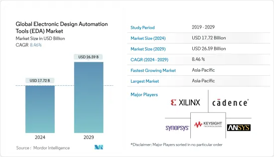
在預測期內(2024-2029),電子設計自動化(EDA)工具的全球市場規模預計到 2024 年為 177.2 億美元,到 2029 年將達到 265.9 億美元。預計將以複合年成長率成長8.46%。
市場擴張背後的主要因素是對小型電子設備的需求不斷成長以及SoC技術在汽車、物聯網和人工智慧等各個行業中的使用不斷增加。
主要亮點
- 近年來,電子設計自動化(EDA)技術使矽領域取得了進展。 EDA 負責以生態系統有利可圖的成本創建 IC 設計流程所需的設計工具。
- 使用 EDA 工具的好處包括減少複雜 IC 開發所需的時間、降低製造成本、消除製造缺陷、改進 IC 設計以及提高易用性。
- 根據世界半導體貿易統計(WSTS),預計2021年半導體產業將成長10.9%,達到約4,880億美元,較前一年增速大幅成長。因此,預計各半導體供應商將增加研發預算。
- 晶片製造商越來越傾向於將人工智慧整合到邊緣運算中。因為邊緣運算在設備層級提供運算能力,從而提高效率和回應時間。例如,英特爾專注於“邊緣運算”,實現人工智慧從物聯網設備到智慧型手機的嵌入。
- EDA 因其許多優點而變得越來越普及,包括減少設計時間和減少錯誤。 EDA 工具已廣泛應用於各種產業,包括汽車和航太產業。然而,EDA 的缺點之一是它不能提供對過去設計的洞察。
- 自半導體誕生以來,莫耳定律(積體電路中電晶體的數量將每 18 至 24 個月增加一倍的預測)一直被遵循。但近年來,科學家開始相信,基本的物理限制可能很快就會使在同一小區域經濟地放置更多元素變得困難,並且莫耳定律可能被證明是錯誤的。
- 自COVID-19爆發以來,半導體產業受到嚴重影響,對供應鏈和生產設備造成重大影響。 2020 年 2 月和 3 月,中國大陸和台灣地區的生產暫停,影響了全球其他OEM生產。然而,很大一部分主要供應商在農曆新年之前儲備了電子設備,這降低了風險。此外,由於半導體產業成長放緩,疫情初期對 EDA 工具的需求略有下降,但這一市場在過去一年中有所成長。
EDA工具市場趨勢
IC物理設計與檢驗領域顯著成長
- IC 物理設計是指使用 EDA 工具建立 IC 的幾何表示。 EDA用於將晶片分類為小塊,並規劃每個區塊所需的特定空間,以確保最大性能。然後使用時鐘合成前後放置這些塊。
- 最近的技術進步鼓勵晶片組製造商利用 ASIC 技術,主要用於 5G。結構化 ASIC 的出現,例如同時具有 ASIC 和現場可編程閘陣列 (FPGA) 元件的架構,導致了成熟的 ASIC 的出現,這導致了與 ASIC 相比更低的製造成本。
- 混合訊號晶片或具有類比和數位電路的積體電路 (IC) 是一種日益成長的趨勢。混合訊號架構對於 SoC 和 ASIC 設計人員來說變得越來越重要。這種需求受到物聯網、通訊、汽車工業、工業控制等產業的影響。例如,2022年7月,西門子EDA(原Mentor)混合訊號檢驗軟體Symphony Pro獲得重大更新。
- 同樣在 2022 年 7 月,Siemens Digital Industries Software 宣佈為積體電路 (IC) 實體檢驗的 Calibre 平台提供電子設計自動化 (EDA) 的各種增強型早期設計檢驗(EDV) 功能。這些新功能的開發旨在透過識別、分析和解決 IC 和系統晶片(SoC) 實體檢驗中的難題,幫助 IC 設計團隊和公司更快地完成計劃。將解決方案移至設計和檢驗的早期階段流程中,我們幫助IC 設計人員「委託」實體和電路檢驗任務。
- 此外,2022年2月,國際知名電子設計服務供應商Veriest Solutions宣布將服務範圍擴大到包括實體設計服務,並在英國建立了一個設計中心。英國的新專家團隊將使該公司的現有客戶和新客戶能夠獲得可測試設計(DFT)和實體設計支援。新團隊還將幫助電子系統公司將整個 ASIC 設計計劃委託給 Veriest,滿足客製化半導體設計高品質解決方案日益成長的需求。
預計北美將佔據較大市場佔有率
- EDA 工具通常用於設計電路基板、處理器和其他複雜的電子設備。隨著EDA工具在家電和汽車等行業的採用,北美市場需求預計將增加。此外,半導體和電路製造業新興市場的開拓正在增加 EDA 工具在該地區的存在。此外,一些主要 EDA 工具供應商的總部位於北美,包括 Xilinx、Ansys、Keysight Technologies、Cadence Design Systems 和 Synopsys。
- 一些北美供應商正在投資擴大其產品線和企業範圍,以滿足該地區對 EDA 工具的需求。例如,晶片製造商 Advanced Micro Devices 於 2022 年 5 月宣布,打算將部分用於晶片設計的電子設計自動化工作負載轉移到 Google Cloud,以擴展其資料中心的功能。這使您可以利用 Google 最新的運算最佳化的 C2D虛擬機實例,該實例由第三代 AMD EPYC 處理器提供支持,並具有先進的網路、儲存和人工智慧功能。
- 一些供應商繼續看到客戶的強勁需求,他們希望加快數位轉型,以應對日益激烈的競爭和更快的上市時間。例如,英特爾代工服務 (IFS) 於 2022 年 7 月宣布了一項全新的雲端聯盟計劃,作為其加速器計劃的一部分。雲端聯盟透過按需運算提高代工客戶的設計效率,同時保護雲端中的設計環境。 Ansys、Cadence、Siemens EDA 和 Synopsys 以及電氣設計自動化 (EDA) 領域的其他知名企業都是雲端聯盟的創始成員。
- 2021年6月,台積電(TSMC)將投資120億美元在亞利桑那州建造電腦晶片工廠,並於2024年開始採用該公司5奈米製造技術大規模生產晶片,打算有所作為。此外,2021年4月,該公司宣布了一項1,000億美元的投資計劃,以在未來三年內增加工廠產能。
- 美國是半導體產業製造、設計和研究的重要國家。該地區的崛起正在推動電子產品的出口需求以及消費性電子產品和汽車行業等最終用戶行業的成長,這些行業是半導體的重要消費者。例如,美國半導體公司半導體產業協會(SIA)2022年2月公佈,2021年全球半導體產業收益達5,559億美元,創歷史最高年度總額,2020年總額為4,404億美元。成長26.2%。由於晶片製造商增加產量以滿足全球晶片短缺帶來的強勁需求,2021年半導體產業出貨達到1.15兆台的歷史新高。
EDA工具產業概況
EDA 市場高度分散。汽車、物聯網、人工智慧和虛擬/擴增實境領域的新商機使半導體公司能夠在 IC 生產週期的各個階段蓬勃發展,從而實現收入的顯著成長。儘管晶片性能顯著提高,但單位銷售價格仍相對持平。該行業的一些主要企業包括 ANSYS、Cadence Design Systems、 摘要和 Keysight Technologies。 EDA 市場的主要發展包括:
- 2022 年 3 月 - Synopsys 宣布推出專為雲端設計的新電子設計自動化 (EDA) 部署模式。該模型透過單一來源、付費使用制提供了「無與倫比的晶片和系統設計彈性」。借助 Microsoft Azure 上預先最佳化的基礎設施,Synopsys Cloud 提供對雲端最佳化設計和檢驗技術的訪問,以解決晶片開發中日益增加的相互依賴性。
- 2021 年 6 月 - Xilinx 宣布推出 Vivado ML Editions,這是一款 FPGA EDA 工具包,可基於機器學習 (ML) 最佳化技術和基於團隊的先進設計程序顯著縮短設計時間和成本。將新的 Vivado ML 版本與現有的 Vivado HLx 版本進行比較,前者的編譯時間加快了五倍,並且在具有挑戰性的設計中實現了突破性的結果品質 (QoR) 平均提高 10%。
- 2021 年 6 月 - Aldec 開始提供 HES-DVM 原型雲端版本 (CE)。 HES-DVM Proto CE 可用於對基於 FPGA 的 SoC/ASIC 設計原型製作,並專注於自動化設計分區,當需要多達四個 FPGA 來容納一個推出時間。
- 2021 年 5 月 - Cadence Design Systems 宣布推出適用於 PCI Express 5.0 規範的低功耗 IP,針對採用台積電 N5 製程技術製造的超大規模運算、網路和儲存應用。此外,PCIe 5.0技術由PHY、伴同性控制器和檢驗IP(VIP)組成,針對適合應用的超高頻寬SoC設計。
其他福利:
- Excel 格式的市場預測 (ME) 表
- 3 個月分析師支持
目錄
第1章簡介
- 研究假設和市場定義
- 調查範圍
第2章調查方法
第3章執行摘要
第4章市場洞察
- 市場概況
- 產業價值鏈分析
- 產業吸引力波特五力分析
- 供應商的議價能力
- 買方議價能力
- 新進入者的威脅
- 競爭公司之間敵對關係的強度
- 替代品的威脅
- 評估 COVID-19 對產業的影響
第5章市場動態
- 市場促進因素
- 汽車、IoT、AI領域的活動
- 具有機器學習功能的 EDA 工具集的趨勢
- 市場限制因素
- 莫耳定律的失敗
第6章市場區隔
- 類型
- 電腦輔助工程(CAE)
- IC物理設計與檢驗
- 印刷基板和多晶片模組(PCB 和 MCM)
- 半導體智慧財產權(SIP)
- 服務
- 目的
- 通訊
- 消費性電子產品
- 車
- 產業
- 其他用途
- 地區
- 北美洲
- 歐洲
- 亞太地區
- 世界其他地區
第7章 競爭形勢
- 公司簡介
- Altium Limited
- Ansys Inc.
- Cadence Design Systems Inc.
- Keysight Technologies Inc.
- Agnisys Inc.
- Aldec Inc.
- Lauterbach GmbH
- Mentor Graphic Corporation(Siemens PLM Software)
- Synopsys Inc.
- Xilinx Inc.
- Zuken Ltd.
第8章投資分析
第9章市場的未來
The Global Electronic Design Automation Tools Market size is estimated at USD 17.72 billion in 2024, and is expected to reach USD 26.59 billion by 2029, growing at a CAGR of 8.46% during the forecast period (2024-2029).
The main factors propelling the market's expansion are the growing need for compact electronic devices and the expanding use of SoC technology across various industries, including automotive, IoT, and AI.
Key Highlights
- The silicon sector has evolved in recent years because of electronic design automation (EDA) techniques. EDA is responsible for creating the design tools necessary for the IC design process at a cost that enables the ecosystem to run profitably.
- Some of the benefits of using EDA tools include reducing the amount of time needed to develop complicated ICs, cutting manufacturing costs, eliminating manufacturing defects, improving IC design and ease of use, etc.
- According to World Semiconductor Trade Statistics (WSTS), the semiconductor industry is expected to grow by 10.9% in 2021, which is a significant growth compared to the previous year's growth, approximately amounting to USD 488 billion. Owing to this, various semiconductor vendors are expected to increase their R&D budgets. For instance, in April 2021, Taiwan Semiconductor Manufacturing Corporation ( TSMC) announced to spend USD 100 billion over the next three years to expand its chip fabrication capacity and R&D.
- Chipmakers are increasingly leaning toward incorporating AI on edge computing, owing to the computational capabilities it brings to the table at the device level, increasing both efficiency and response time. For instance, Intel is focusing on 'edge computing' to enable AI incorporation into IoT devices to smartphones.
- EDA has become more popular due to its many benefits, including shorter design times and fewer errors. EDA tools have become more widely used in various industries, including the automotive and aerospace industries. However, one of EDA's shortcomings lies in its inability to obtain insights from previous designs.
- Since the inception of semiconductors, Moore's Law-the prediction that the number of transistors in an integrated circuit will increase two-fold every 18-24 months-has held true. However, in recent years, scientists have increasingly come to believe that fundamental physical limits may soon make it hard to economically place additional elements on the same small area, which could ultimately prove that Moore's Law is faulty.
- Since the COVID-19 breakout, the semiconductor industry has been severely impacted, significantly impacting its supply chain and production facilities. In February and March 2020, China and Taiwan's production ceased, affecting other OEM production worldwide. However, a significant portion of important vendors stocked up on electronics in anticipation of the Chinese New Year, which reduced the risk. Additionally, with the semiconductor industry's slowing growth, the initial pandemic epidemic saw a minor decline in demand for EDA tools; but, over the course of a year, the market experienced growth.
EDA Tools Market Trends
IC Physical Design and Verification Segment to Grow Significantly
- IC physical design refers to the creation of geometric representations of ICs, using EDA tools. EDA is used to divide the chip into smaller blocks and then plan the specific space required for each block to ensure maximum performance. These blocks are then placed, using before and after clock synthesis.
- The recent technological advancements have been helping several chipset manufacturers to make use of ASIC technology, mainly for 5G. The advent of structured ASIC, having elements of both ASICs and field-programmable gate arrays (FPGA), like architecture, has led to the cost of production becoming cheaper compared to full-blown ASIC, which requires the addition of a modifiable on top of the base ASIC layer.
- Mixed-signal chips, or integrated circuits (ICs) featuring analog and digital circuitry, are a growing trend. Mixed-signal architectures are becoming progressively and more necessary for SoC and ASIC designers. This demand is influenced by industries including the internet of things, communications, the automobile industry, and industrial control. For instance, in July 2022, the mixed-signal verification software Symphony Pro had a significantly updated version from Siemens EDA (previously Mentor).
- Also, in July 2022, Siemens Digital Industries Software announced a variety of expanded early design verification (EDV) functions for electronic design automation (EDA) for its Calibre platform for integrated circuit (IC) physical verification. These new capabilities, which were developed to assist IC design teams and businesses in completing projects more quickly, can assist IC designers in "shifting left" their physical and circuit verification tasks by putting the identification, analysis, and resolution of challenging IC and system-on-chip (SoC) physical verification issues into earlier stages of the design and verification flow.
- Furthermore, in February 2022, Veriest Solutions, a prominent international provider of electronics design services, built a design center in the United Kingdom and announced the expansion of its offerings to include physical design services. Customers of the company, both current and new, will now have access to Design for Test (DFT) and Physical Design support due to the new specialist team in the United Kingdom. The inclusion of the new team will also allow electronic system firms to outsource whole ASIC design projects to Veriest, meeting the growing need for high-quality solutions for customized semiconductor designs.
North America is Expected to Hold a Significant Market Share
- EDA tools often design circuit boards, processors, and other complex electronics. The adoption of EDA tools in industries such as consumer electronics, and automotive, is set to increase demand for the market in North America. Also, growing developments in the semiconductor industry and circuit manufacturing industry have raised the market's prominence in the region. Also, some of the significant vendors of EDA tools are headquartered in North America, such as Xilinx Inc., Ansys Inc., Keysight Technologies Inc., Cadence Design Systems Inc., and Synopsys Inc.
- Some North American suppliers have been investing in improving the company's product lines and broadening the firm reach to meet the demand for EDA tools in the region. For instance, in May 2022, Chipmaker Advanced Micro Devices Inc. announced that the company intends to move some of its electronic design automation workloads for chip design onto Google Cloud to expand the capabilities of the company's data centers. This will allow taking advantage of Google's most recent compute-optimized C2D virtual machine instances, which are powered by 3rd Gen AMD EPYC processors, as well as advanced networking, storage, and artificial intelligence capabilities.
- Some of the vendors have continued to see strong demand from their customers, who are looking forward to accelerating their digital transformation as engineering teams adapt to increasing competition and shrinking time to market windows. For instance, in July 2022, Intel Foundry Services (IFS) unveiled a brand-new Cloud Alliance program as a component of its Accelerator program. Cloud Alliance streamlines design efficiency for foundry clients with on-demand computing while securing design environments on the cloud. Ansys, Cadence, Siemens EDA, and Synopsys are a few of the founding members of the Cloud Alliance, along with other prominent companies in electrical design automation (EDA).
- In June 2021, Taiwan-based Semiconductor Manufacturing Co. Ltd (TSMC) started construction at a site in Arizona where it plans to spend USD 12 billion to build a computer chip factory, which will begin volume production of chips using the company's 5-nanometer production technology starting in 2024. The company also announced a USD 100 billion investment plan in April 2021 to increase capacity at its factories over the next three years.
- The United States is a significant country in the semiconductor industry's manufacturing, design, and research. The region's prominence drives the demand for exporting electronics equipment and growing end-user industries that are significant consumers of semiconductors, such as consumer electronics and the automotive industry. For instance, the US semiconductor company, the Semiconductor Industry Association (SIA), in February 2022, reported that revenues for the worldwide semiconductor industry reached USD 555.9 billion in 2021, the highest yearly total ever and a rise of 26.2% over the USD 440.4 billion total for 2020. In 2021, the semiconductor industry shipped a record 1.15 trillion units as chip companies increased output to meet the strong demand brought on by the worldwide chip shortage.
EDA Tools Industry Overview
The EDA market is highly fragmented. New opportunities in the automotive, IoT, artificial intelligence and virtual/augmented reality sectors have allowed semiconductor companies throughout all phases of the IC production cycle to prosper, with sizable revenue increases. This has occurred despite significant gains in chip performance but at relatively flat unit sales prices. Some of the key players in the industry include ANSYS, Cadence Design Systems, Synopsis, Keysight Technologies, etc. Some of the key developments in the EDA market are as follows:
- March 2022 - Synopsys has announced the introduction of a new electronic design automation (EDA) deployment model that is designed for the cloud and provides "unparallel levels of chip and system design flexibility" through a single-source, pay-as-you-go approach. With pre-optimized infrastructure on Microsoft Azure, Synopsys Cloud provides access to the company's cloud-optimized design and verification technologies, which address increased levels of interdependencies in chip development.
- June 2021 - Xilinx, Inc. unveiled Vivado ML Editions, an FPGA EDA tool package based on machine learning (ML) optimization techniques and advanced team-based design procedures for considerable design time and cost savings. Comparing the new Vivado ML Editions to the existing Vivado HLx Editions, the former offers a 5x quicker compilation time and revolutionary quality of results (QoR) improvements that average 10% on difficult designs.
- June 2021 - Aldec Inc. launched HES-DVM Proto Cloud Edition (CE). It is available through Amazon Web Service (AWS); HES-DVM Proto CE can be used for FPGA-based prototyping of SoC / ASIC designs and focuses on automated design partitioning to greatly reduce bring-up time when up to four FPGAs are needed to accommodate a design.
- May 2021- Cadence Design Systems announced low-power IP for the PCI Express 5.0 specification that targets hyper-scale computing, networking, and storage applications that are made on TSMC N5 process technology. In addition, PCIe 5.0 technology consists of a PHY, companion controller, and Verification IP (VIP) targeted at SoC designs for very high bandwidth to suit the applications.
Additional Benefits:
- The market estimate (ME) sheet in Excel format
- 3 months of analyst support
TABLE OF CONTENTS
1 INTRODUCTION
- 1.1 Study Assumptions and Market Definition
- 1.2 Scope of the Study
2 RESEARCH METHODOLOGY
3 EXECUTIVE SUMMARY
4 MARKET INSIGHTS
- 4.1 Market Overview
- 4.2 Industry Value Chain Analysis
- 4.3 Industry Attractiveness: Porter's Five Forces Analysis
- 4.3.1 Bargaining Power of Suppliers
- 4.3.2 Bargaining Power of Buyers
- 4.3.3 Threat of New Entrants
- 4.3.4 Intensity of Competitive Rivalry
- 4.3.5 Threat of Substitute Products
- 4.4 Assessment of the Impact of COVID-19 on the Industry
5 MARKET DYNAMICS
- 5.1 Market Drivers
- 5.1.1 Booming Automotive, IoT, and AI Sectors
- 5.1.2 Upcoming Trend of EDA Toolsets Equipped with Machine Learning Capabilities
- 5.2 Market Restraints
- 5.2.1 Moore's Law about to be Proven Faulty
6 MARKET SEGMENTATION
- 6.1 Type
- 6.1.1 Computer-aided Engineering (CAE)
- 6.1.2 IC Physical Design and Verification
- 6.1.3 Printed Circuit Board and Multi-chip Module (PCB and MCM)
- 6.1.4 Semiconductor Intellectual Property (SIP)
- 6.1.5 Services
- 6.2 Application
- 6.2.1 Communication
- 6.2.2 Consumer Electronics
- 6.2.3 Automotive
- 6.2.4 Industrial
- 6.2.5 Other Applications
- 6.3 Geography
- 6.3.1 North America
- 6.3.2 Europe
- 6.3.3 Asia Pacific
- 6.3.4 Rest of the World
7 COMPETITIVE LANDSCAPE
- 7.1 Company Profiles
- 7.1.1 Altium Limited
- 7.1.2 Ansys Inc.
- 7.1.3 Cadence Design Systems Inc.
- 7.1.4 Keysight Technologies Inc.
- 7.1.5 Agnisys Inc.
- 7.1.6 Aldec Inc.
- 7.1.7 Lauterbach GmbH
- 7.1.8 Mentor Graphic Corporation (Siemens PLM Software)
- 7.1.9 Synopsys Inc.
- 7.1.10 Xilinx Inc.
- 7.1.11 Zuken Ltd.
8 INVESTMENT ANALYSIS
9 FUTURE OF THE MARKET
 2024 年全球電子設計自動化 (EDA) 工具市場報告
 2024 年雲端 EDA(電子設計自動化)全球市場報告
 2024 年電子設計自動化 (EDA) 全球市場報告
 全球電子設計自動化軟體市場規模、佔有率、成長分析(按應用、按產品提供)- 2024-2031 年產業預測
 2024-2032 年按解決方案類型(半導體 IP、CAE、IC 物理設計和驗證、PCB 和 MCM、服務)、部署類型、最終用途行業和地區分類的電子設計自動化市場報告
 電子設計自動化軟體市場,按產品類型、部署、按應用、最終用戶、國家和地區 - 2023-2030 年行業分析、市場規模、市場佔有率和預測
 光子設計自動化市場規模和預測、全球和地區佔有率、趨勢和成長機會分析報告範圍:按組件、部署、組織規模和應用
 電子設計自動化軟體全球市場報告 2024年
 電子設計自動化 (EDA) 市場 - 按產品(電腦輔助工程、IC 物理設計和驗證、印刷電路板和多晶片模組、半導體智慧財產權、服務)、按應用和預測,2023 年至 2032 年
 電子設計自動化 (EDA) 軟體市場報告:2030 年趨勢、預測與競爭分析