


 |
市場調查報告書
商品編碼
1406267
半導體光刻設備:市場佔有率分析、產業趨勢與統計、2024年至2029年成長預測Semiconductor Lithography Equipment - Market Share Analysis, Industry Trends & Statistics, Growth Forecasts 2024 - 2029 |
||||||
※ 本網頁內容可能與最新版本有所差異。詳細情況請與我們聯繫。
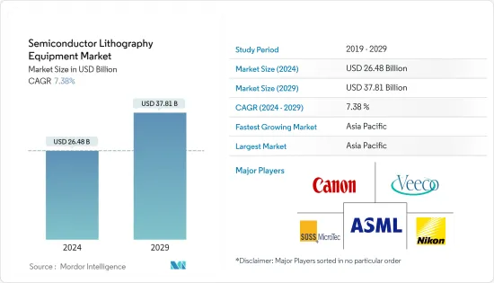
預計2024年半導體光刻設備市場規模為264.8億美元,2029年預計將達378.1億美元,在預測期內(2024-2029年)複合年成長率為7.38%。
主要亮點
- 由於廣泛應用於消費性電子和汽車等幾乎所有領域的半導體裝置製造規模的擴大,全球半導體光刻設備市場預計將成長。智慧型設備的採用正在不斷增加,並且預計隨著 5G 連接和採用在全球範圍內的普及,智慧型設備的採用也會不斷成長。根據GSMA預測,2025年5G行動寬頻連線預計將達到11億,到2025年5G普及預計將覆蓋全球34%的人口。
- 超過50%的半導體FAB(製造)成本來自於設備和工具。光刻是推進半導體製造製程的設備之一。半導體製造的多個方面都依賴光刻設備。從技術角度來看,產量比率和缺陷就是兩個這樣的例子。這是半導體製造如此關注採用哪種類型的光刻技術的主要原因。
- 隨著半導體產品變得越來越複雜,缺陷的類型也越來越複雜。然而,光刻設備被設計用來處理這個複雜的過程。隨著半導體製造商專注於下一代先進技術節點,無錯誤光刻設備變得更加重要。
- 此外,隨著 5G 和物聯網連接設備的出現,製造業最近經歷了顯著成長,預計將促進無線控制等各種工業 4.0 應用所需的連接。這對於移動工具、機械和機器人尤其重要,可以幫助預測期內的市場成長。
- 多家產業公司致力於為各種應用提供新型光刻系統。例如,尼康公司將於2022年3月推出全新第8代平板FPD光刻系統,該系統將支援高階顯示器、大型電視和智慧型手機等高付加優質顯示器的各種高畫質面板的生產。設備. 宣布.
- 半導體產業是最複雜的產業之一,擁有 500 多個製造和測試流程。因此,根據製造流程的複雜程度,半導體晶圓的完整製造和檢驗大約涉及1,400個步驟。這一複雜的過程對市場成長構成了顯著的障礙。
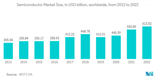
- 相反,在對下一代電子產品的強勁需求的支持下,COVID-19 大流行使資本設備產業持續成長。 SEMI 的數據顯示,2021 年全球半導體製造設備銷售額激增 44%,達到 1,026 億美元,高於去年同期的 712 億美元。
半導體光刻設備市場趨勢
深紫外光刻(DUV)佔據主要市場佔有率
- 深紫外光刻 (DUV) 是一種光學投影微影技術,其中光罩上的圖案透過 4 倍或 5 倍光學元件投影到晶圓表面。這種類型的光刻所使用的波長是248nm或193nm。這種微影技術是一種高速微影技術,非常適合對 22mm x 22mm 以下的分立元件進行大面積母版處理,22mm x 22mm 是 DUV 工具的典型晶圓級曝光場尺寸。
- DUV光刻類型是具有代表性的下一代光刻技術之一。該技術具有成本效益,並提供更高的解析度。 DUV 微影技術的採用主要是由小型化趨勢所推動的。光刻用於在半導體晶圓上印刷表徵積體電路 (IC) 的複雜圖案。
- DUV 微影可以輕鬆創建低功耗的輕量電子晶片。該平台提供了改進的功率解析度並且具有成本效益。這些結構一起形成一個 IC,稱為晶片。半導體產業對更高效微晶片的追求意味著晶片製造商需要研究晶片上的更多結構,使其速度更快、效率更高,同時降低製造成本。預計這將推動預測期內的市場成長。
- ASML 表示,向 EUV 的過渡可能會進一步增加對 DUV 的需求。晶片製造商在晶片製造的早期階段引入EUV,應用電晶體、最小通孔(將源極、閘極和汲極連接到複雜互連層的接點)等微結構,以及在某些情況下的連接層。
- 隨著公司尋求能夠製造高達 7 奈米節點晶片的技術,市場正在見證各種投資。例如,Canon於2022年10月宣布將在日本東部建立新的半導體設備工廠,生產半導體光刻設備等產品。該設施預計將於 2025 年上半年運作。
- 領先供應商的此類市場開拓以及政府提高半導體產量的舉措預計將在預測期內推動市場成長。
美國佔有很大佔有率
- 美國擁有強大的半導體研發能力,大量投資擴大半導體製造能力,快速引進尖端技術。
- 此外,美國對半導體的需求正在增加。例如,根據2021年9月世界半導體貿易統計數據(WSTS),2021年半導體產業銷售額大幅成長至5,270億美元,主要得益於2020年整個市場需求成長強勁。該預測已上修。 WSTS 預測 2022 年全球銷售額將達到 5,730 億美元。
- 此外,根據半導體設備與材料國際公司的數據,2022 年 4 月,北美半導體設備支出在 2021 年達到 76.1 億美元,而 2020 年為 65.3 億美元。
- 半導體產業團體也表示,美國半導體產業在晶片設計方面處於領先地位。美國無廠半導體公司約佔全球無廠半導體公司銷售額的60%,安排無晶圓廠銷售額的一些最大的IDM都是美國公司。
- 根據美國半導體產業的狀況,2019年運行在半導體晶片上的連網型設備(ioT:物聯網)價值達到226億美元,預計到2025年將達到750億美元。半導體也是 3D 列印、機器學習和人工智慧 (AI) 等創新的基礎,這些創新可改善醫療保健、降低建築成本、增強食品供應並促進科學進步。該地區對半導體的強勁需求可能會推動預測期內半導體光刻設備的採用。
- 此外,2022年9月,拜登政府宣布美國將發展國內半導體產業,以對抗對中國的依賴,因為美國零產量,只消費量了全球最先進晶片的25%,而這些晶片對於美國來說至關重要。為了國家安全,宣布將投資500億美元拜登總統於 2022 年 8 月簽署了 2800 億美元的 CHIPS 法案,以促進國內高科技製造業,作為增強美國對中國競爭力的努力的一部分。該地區半導體行業如此強勁的投資可能會為研究市場的成長提供利潤豐厚的機會。
半導體光刻設備產業概況
該市場集中在 ASML、Veeco 和 Nikon 等少數供應商手中。半導體製造的主要設備基本上被美國和日本企業壟斷。由於整合不斷增加、技術進步和地緣政治形勢,所研究的市場正在經歷波動。此外,隨著垂直整合的推進,考慮到投資與收益的匹配能力,市場競爭預計將繼續加劇。
- 2022年9月-Canon發布半導體光刻設備解決方案平台「Lithography Plus1」。將Canon50多年的半導體光刻設備支援經驗和大量資料融入系統中,以最大限度地提高支援效率,並提案並實現最佳的系統流程。
- 2022 年 6 月 - 三星和 ASML 同意合作開發 High-NA(高數值孔徑)EUV 光刻設備,並於明年開始銷售。與傳統 EUV 微影設備相比,新一代高數值孔徑 EUV 微影設備可以形成更小的電路。
其他福利:
- Excel 格式的市場預測 (ME) 表
- 3 個月分析師支持
目錄
第1章簡介
- 研究假設和市場定義
- 調查範圍
第2章調查方法
第3章執行摘要
第4章市場洞察
- 市場概況
- 產業吸引力-波特五力分析
- 供應商的議價能力
- 買方議價能力
- 新進入者的威脅
- 替代品的威脅
- 競爭公司之間的敵對關係
- 半導體光刻設備技術藍圖
- 宏觀經濟走勢對市場的影響
第5章市場動態
- 市場促進因素
- 由於電動車和先進的移動設備,對更小尺寸和更高功能的需求不斷增加
- 專業設備供應商提供新型光刻設備,技術創新進步
- 市場抑制因素
- 製造過程中與圖案複雜性相關的課題
第6章市場區隔
- 類型
- 深紫外光微影 (DUV)
- 極紫外光刻(EUV)
- 目的
- 先進封裝
- 微機電系統元件
- LED元件
- 地區
- 北美洲
- 歐洲
- 亞太地區
- 世界其他地區
第7章 競爭形勢
- 公司簡介
- Canon Inc.
- Nikon Corporation
- ASML Holding NV
- Veeco Instruments Inc.
- SUSS MicroTec SE
- Shanghai Micro Electronics Equipment(Group)Co. Ltd
- EV Group(EVG)
- JEOL Ltd
- Onto Innovation(Rudolph Technologies Inc.)
- Neutronix Quintel Inc.(NXQ)
- 供應商市場佔有率分析
第8章投資分析
第9章市場的未來
The Semiconductor Lithography Equipment Market size is estimated at USD 26.48 billion in 2024, and is expected to reach USD 37.81 billion by 2029, growing at a CAGR of 7.38% during the forecast period (2024-2029).
Key Highlights
- The global semiconductor lithography equipment market is expected to grow with the growing manufacturing of semiconductor devices that are widely used in nearly all sectors including consumer electronics, automotive, and many others. Smart device adoption is increasing and is expected to grow as 5G connections and adoption spread over the globe. As per GSMA, 5G mobile broadband connections are expected to reach 1,100 million by 2025, with the 5G rollout expected to cover 34 percent of the world's population by 2025.
- More than 50 percent of the semiconductor FAB (fabrication) cost is due to equipment and tools. One piece of equipment that drives the semiconductor fabrication process forward is lithography. There are several aspects of semiconductor fabrication that has driven by lithography equipment. Yield and defect are two such examples from the technical point of view. It is the primary reason why semiconductor fabrication focuses a lot on which type of lithography technology to deploy.
- With the rising complexity in semiconductor products, the types of defects are also getting complex. However, lithography equipment is supposed to handle the complex process. With semiconductor manufacturers focusing on next-gen advanced technology nodes, the importance of error-free lithography equipment is significantly increasing further.
- Moreover, manufacturing businesses are are lately growing at a signficant rate with the advent of 5G and emergence of IoT connected devices, which is anticipated to facilitate the connection required for various Industry 4.0 applications, such as wireless control. This is especially essential for mobile tools, machines, and robots that can aid market growth during the forecast period.
- Several industry players are focusing on offering new lithography systems to serve a wide range of applications. For instance, in March 2022, Nikon Corporation announced to launch new Gen 8 plate FPD lithography system to support the production of various high-definition panels for value-added premium displays, such as high-end monitors, large TVs, and smart devices.
- The semiconductor industry is considered as one of the most complex industries, not only owing to the presence of more than 500 processing steps involved in the manufacturing and inspection and various products but also due to the harsh environment it goes through, e.g., the volatile electronic market and the unpredictable demand. Therefore, depending on the intricacy of the manufacturing process, there are about 1,400 process steps in the complete manufacturing and inspection of semiconductor wafers alone. Such a complex process poses a notable hurdle to the market's growth.
- On the contrary, the COVID-19 pandemic kept the capital equipment sector growing with a strong demand for next-generation electronics. As per SEMI, the global sales of semiconductor manufacturing equipment surged by 44 percent in 2021 to a record of USD 102.6 billion, up from USD 71.2 billion in the previous year.
Semiconductor Lithography Equipment Market Trends
Deep Ultraviolet Lithography (DUV) to Hold Major Market Share
- Deep UV lithography (DUV) is an optical projection lithography technique where the pattern on the mask is projected to the wafer surface through a 4X or 5X optical system. The wavelengths used for this type of lithography are 248 nm or 193 nm. This lithography is a high-speed lithographic technology ideal for large-area masters of discrete components that are not bigger than 22 mm x 22 mm, the typical wafer-level exposure field size of a DUV tool.
- The DUV lithography type is one of the leading lithography technologies of the next generation. The technology is cost-effective and has increased resolving power. The adoption of DUV lithography is driven primarily by the miniaturization trend. Lithography is used for printing complex patterns that characterize integrated circuits (ICs) on semiconductor wafers.
- Using DUV lithography, lightweight electronic chips with lower power demands are easy to achieve. The platform features enhanced power resolution and is cost-effective. These structures together form an IC, which is known as a chip. The semiconductor industry's search for even more efficient microchips means chipmakers have to study more structures onto a chip, making the chip faster and more efficient while also reducing production costs. This is expected to boost the market's growth over the forecast period.
- According to ASML, a transition to EUV may only boost demand for DUV. Chip manufacturers deploy EUV in the early stages of chip fabrication to apply the minor structures: transistors, smallest vias (the contacts that connect the source, gate, and drain to the complex interconnect layers), and possibly the connecting layer.
- The market is witnessing various investments as the companies are seeking a technology that can produce chips down to 7nm nodes. For instance, in Oct 2022, Canon announced the development of a new semiconductor equipment plant in eastern Japan which will produce semiconductor lithography systems and other devices. The facilities are expected to commence operation by the first half of 2025.
- Such developments by the major vendors, along with the initiatives taken by the government to boost their semiconductor production, are expected to drive market growth over the forecast period.
United States to Witness Significant Share
- The United States boasts robust semiconductor R&D capabilities, significant investments catering to the expansion of semiconductor manufacturing capabilities, and rapid adoption of advanced technologies.
- Further, the United States is witnessing an increasing demand for semiconductors. For instance, in September 2021, according to the world semiconductor trade statistics (WSTS), semiconductor industry sales increased significantly to USD 527 billion in 2021, an upward revision from the 2020 forecast for 2021 due mainly to the strong demand growth in the overall market 2020. In 2022, WSTS forecasted global sales totaled to USD 573 billion.
- Additionally, in April 2022, according to Semiconductor Equipment and Materials International, North America's spending on semiconductor equipment reached USD 7.61 billion in 2021 compared to 2020, which was USD 6.53 billion.
- Also, the semiconductor industry association stated that the US semiconductor industry is a leader in chip design. The United States fabless firms account for roughly 60 percent of all global fabless firm sales, and some of the largest IDMs, which make their arrangement, are also US firms.
- According to the state of the US semiconductors industry, the connected devices that run on semiconductor chips (i.e., the Internet of Things (IoT)) registered USD 22.6 billion in 2019 and are expected to reach USD 75 billion by 2025. Semiconductors are also fundamental to innovations, such as 3D printing, machine learning, and artificial intelligence (AI) that enhance healthcare, reduce building costs, strengthen food supply, and enable advancements in science. The region's robust semiconductor demand is likely to boost the adoption of semiconductor lithography equipment during the forecast period.
- Additionally, in September 2022, the Biden administration announced that it would invest USD 50 billion in building up the domestic semiconductor industry to counter dependency on China, as the US produces zero and consumes 25 percent of the world's leading-edge chips vital for its national security. President Joe Biden signed a USD 280 billion CHIPS bill in August 2022 to boost domestic high-tech manufacturing, part of his administration's push to boost US competitiveness over China. Such robust investments in the semiconductor sector in the region would offer lucrative opportunities for the growth of the studied market.
Semiconductor Lithography Equipment Industry Overview
The market is concentrated due to a few vendors such as ASML, Veeco, and Nikon occupying the majority market share. The key equipment for semiconductor manufacturing is basically monopolized by American and Japanese companies. With growing consolidation and technological advancement, and geopolitical scenarios, the studied market is witnessing fluctuation. In addition, with increasing vertical integration, the intensity of competition in the studied market is expected to continue to rise, considering their ability to invest, which results from their revenues.
- September 2022 - Canon Inc. launched the "Lithography Plus1" solution platform for semiconductor lithography systems. Canon's more than 50 years of experience in semiconductor lithography system support and the company's vast wealth of data are incorporated into the system to maximize support efficiency and propose and implement optimized system processes.
- June 2022 - Samsung and ASML have agreed to collaborate on developing High-NA (high numerical aperture) EUV Lithography equipment, which will be available next year. Compared to older EUV Lithography equipment, the next-generation High-NA EUV Lithography equipment can engrave finer circuits.
Additional Benefits:
- The market estimate (ME) sheet in Excel format
- 3 months of analyst support
TABLE OF CONTENTS
1 INTRODUCTION
- 1.1 Study Assumptions and Market Definition
- 1.2 Scope of the Study
2 RESEARCH METHODOLOGY
3 EXECUTIVE SUMMARY
4 MARKET INSIGHTS
- 4.1 Market Overview
- 4.2 Industry Attractiveness - Porter's Five Forces Analysis
- 4.2.1 Bargaining Power of Suppliers
- 4.2.2 Bargaining Power of Buyers
- 4.2.3 Threat of New Entrants
- 4.2.4 Threat of Substitute Products
- 4.2.5 Intensity of Competitive Rivalry
- 4.3 Semiconductor Lithography Equipment Technology Roadmap
- 4.4 The impact of macroeconomic trends on the Market
5 MARKET DYNAMICS
- 5.1 Market Drivers
- 5.1.1 Increasing Demand for Miniaturization and Extra Functionality by Electric Vehicles and Advanced Mobile Devices
- 5.1.2 Growing Innovation by Specialist Equipment Vendors offering Brand New Lithography Tools
- 5.2 Market Restraints
- 5.2.1 Challenges Regarding Complexity of Pattern in Manufacturing Process
6 MARKET SEGMENTATION
- 6.1 Type
- 6.1.1 Deep Ultraviolet Lithography (DUV)
- 6.1.2 Extreme Ultraviolet Lithography (EUV)
- 6.2 Application
- 6.2.1 Advanced Packaging
- 6.2.2 MEMS Devices
- 6.2.3 LED Devices
- 6.3 Geography
- 6.3.1 North America
- 6.3.2 Europe
- 6.3.3 Asia Pacific
- 6.3.4 Rest of the World
7 COMPETITIVE LANDSCAPE
- 7.1 Company Profiles*
- 7.1.1 Canon Inc.
- 7.1.2 Nikon Corporation
- 7.1.3 ASML Holding NV
- 7.1.4 Veeco Instruments Inc.
- 7.1.5 SUSS MicroTec SE
- 7.1.6 Shanghai Micro Electronics Equipment (Group) Co. Ltd
- 7.1.7 EV Group (EVG)
- 7.1.8 JEOL Ltd
- 7.1.9 Onto Innovation (Rudolph Technologies Inc.)
- 7.1.10 Neutronix Quintel Inc. (NXQ)
- 7.2 Vendor Market Share Analysis


