


 |
市場調查報告書
商品編碼
1433926
扇出封裝:市場佔有率分析、產業趨勢與統計、成長預測(2024-2029)Fan Out Packaging - Market Share Analysis, Industry Trends & Statistics, Growth Forecasts (2024 - 2029) |
||||||
※ 本網頁內容可能與最新版本有所差異。詳細情況請與我們聯繫。
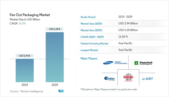
扇出封裝市場規模預計到 2024 年為 29.4 億美元,預計到 2029 年將達到 63 億美元,在預測期內(2024-2029 年)複合年成長率為 16.5%
該市場的擴張是由半導體技術的進步和各行業需求的快速成長所推動的。
主要亮點
- 由於對高性能、節能、薄型和小尺寸封裝的要求,扇出晶圓層次電子構裝(FOWLP) 在智慧型手機等佔地面積敏感的設備中得到越來越多的使用。此外,現代智慧型手機平均採用 5-7 個晶圓級封裝(尤其是扇出封裝),而且這一數字預計未來還會增加。這是因為傳統的堆疊封裝(PoP)記憶體邏輯解決方案正在逐漸被取代。
- 此外,人工智慧和機器學習在各個領域的應用不斷增加,也增加了高效能運算在市場上的採用。超高清扇出技術預計將應用於雲端、5G、自動駕駛汽車和人工智慧晶片,並將在預測期內引領封裝趨勢。
- 韓國半導體產業正在努力改進並使 3D TSV(矽穿孔)、封裝、FoWLP(扇出晶圓級封裝)和 FoPLP(扇出面板級封裝)技術更加有效。提高半導體性能,提高整合度。
- 2021 年 12 月,Nepes Laweh Corporation 宣布已利用 Deca 的 M 系列扇出技術成功製造出全球首款 600 mm x 600 mm 大型面板級封裝 (PLP)。根據該公司介紹,扇出面板級封裝(FOPLP)線已於第三季通過客戶認證,建立穩定的產量比率,並開始全面量產。
- 由於韓國公司迄今為止在這些系統上依賴外國公司,KOSTEK 預計未來進口替代效應將顯著。在扇出封裝過程中可以使用臨時晶圓鍵合機和脫鍵合技術。
- 由於冠狀病毒感染疾病(COVID-19)的爆發,由於貨物流動受到限制以及半導體供應鏈的嚴重中斷,半導體封裝市場成長放緩。 2020 年第一季,COVID-19 降低了半導體供應商和分銷通路客戶的存量基準。新型冠狀病毒的傳播預計將對市場產生長期影響。
扇出型封裝市場趨勢
透過高密度扇出獲得較大佔有率
- 高中階扇出,適用於每平方毫米 6 至 12 個 I/O 和 15/15μm 至 5/5μm 線路/空間的中端到高階應用。高密度扇出封裝已變得流行,以適應行動電話封裝的外形尺寸和性能要求。此技術的主要組成部分包括線路重布(RDL)金屬和巨型柱電鍍。
- 台積電的 InFO 技術是高密度扇出最著名的例子之一。此技術針對高引腳數應用,例如應用處理器 (AP)。該公司計劃將其 FO-WLP 領域擴展到 inFO-Antenna-in-Package (AiP) 和 inFO-on-Substrate 等技術。這些包裝用於汽車、伺服器、智慧型手機等。蘋果是這項新技術的早期採用者之一,在 2016 年底發布的 iPhone 7 的 A10 應用處理器中使用了該技術。
- 由於這些優勢,高通和聯發科於 2021 年 12 月宣布,將採用扇出 PoP 來製造其旗艦智慧型手機應用處理器,效仿蘋果採用台積電 InFO_PoP 技術封裝其 iPhone 晶片的腳步。
- 此外,半導體市場的成長以及高密度扇出封裝解決方案的發展預計將推動預測期內的市場成長。例如,2021年7月,全球領先的複合電路製造商和技術解決方案供應商長電科技正式推出了其用於XDFOI晶片的全系列超高密度扇出封裝選項。一種有效的、高密度連接、高密度、高可靠性的晶片異構整合解決方案。
- 高密度扇出晶圓層次電子構裝(FOWLP) 的生產也取得了進展。正在開發的解決方案旨在縮小晶片尺寸/高度並降低製造成本,同時提高可靠性、能源效率、設備速度和多功能整合。例如,SPTS Technologies 為領先的半導體封裝公司提供多種等電漿蝕刻和沈積製程技術,用於高密度扇出晶圓級封裝等先進封裝方案。
- 此外,晶圓級處理的製造能力與使用高銅 (Cu) 柱和直通封裝等貫穿模製互連件創建 3D 結構的能力相結合,使高密度扇出 (HDFO) 封裝成為可能。 ,可以滿足這些小型化的需求。過孔(TPV)和先進的覆晶構裝技術。
台灣佔有較大市場佔有率
- 台灣是許多主要半導體製造公司的所在地,推動了對先進半導體封裝(尤其是 PLP)的需求。據政府智庫科技國際戰略中心稱,2021年台灣的產出預計將成長25.9%,達到1,470億美元。
- 根據半導體行業協會 (SIA) 的數據,亞太地區的半導體銷售額佔全球半導體銷售額的 50% 以上。這使台灣供應商有機會為越來越多的半導體應用提供 FOWLP。
- 國內大部分企業都擴大了扇出型封裝產能,可望進一步增加出口,有利於開拓國內市場。例如,最近宣布重返晶圓代工廠產業的英特爾也將在新墨西哥州投資35億美元建造半導體封裝工廠,計劃於2022年下半年開始運作。
- 此外,2021年6月,純半導體後處理(OAST)公司日月光開始投資先進封裝設備,以應對半導體供需短缺的情況。我們透過從HANMI Semiconductor購買大量用於WLP和PLP製程的半導體製造設備來加速我們的業務擴張。
- 此外,第五代 (5G) 無線通訊和高效能運算市場的成長使製造商能夠開發新技術。例如,作為高密度扇出領域的唯一領導者,台積電計劃將 FO-WLP 領域擴展到 inFO-天線封裝 (AiP) 和 inFO-on-Substrate (oS) 等技術。
扇出型封裝產業概述
市場適度分散,參與者多。全球扇出型封裝市場的主要企業包括台積電、江蘇長電、Amkor Technology Inc.、三星馬達、力成科技等。這些參與者熱衷於產品創新、併購和收購等發展,以增加市場佔有率。
- 2021 年 11 月 - 半導體封裝和測試服務供應商 Amkor Technology, Inc. 宣布有意在越南北寧省建設智慧工廠。提案工廠的初始階段將專注於為世界領先的半導體和電子製造公司提供先進的系統級封裝(SiP)組裝和測試服務。
- 2021 年 2 月 - 三星晶圓代工廠已向亞利桑那州、紐約州和德克薩斯當局提交文件,尋求在美國建立最先進的半導體製造工廠。該工廠可能建在德克薩斯州奧斯汀附近,預計耗資超過 170 億美元,並創造 1,800 個就業機會。預計2023年第四季上線。
其他福利
- Excel 格式的市場預測 (ME) 表
- 3 個月分析師支持
目錄
第1章簡介
- 研究假設和市場定義
- 調查範圍
第2章調查方法
第3章執行摘要
第4章市場洞察
- 市場概況
- 產業吸引力-波特五力分析
- 供應商的議價能力
- 買方議價能力
- 新進入者的威脅
- 競爭公司之間的敵對關係
- 替代品的威脅
- COVID-19 對市場的影響
第5章市場動態
- 市場促進因素
- 高效能運算和5G無線網路的普及
- 市場限制因素
- 與製造相關的製造成本問題
- FOPLP市場機遇
- COVID-19 對市場的影響
第6章市場區隔
- 按類型
- 核心扇出
- 高密度扇出
- 超密集扇出
- 依營運商類型
- 200 mm
- 300 mm
- 控制板
- 按經營模式
- OSAT
- 鑄造廠
- IDM
- 按地區
- 台灣
- 中國
- 美國
- 韓國
- 日本
- 歐洲
第7章 扇出封裝廠商排名分析
第8章 競爭形勢
- 公司簡介
- Taiwan Semiconductor Manufacturing Company Limited
- Jiangsu Changjiang Electronics Tech Co.
- Samsung Electro-Mechanics
- Powertech Technology Inc.
- Amkor Technology Inc.
- Advanced Semiconductor Engineering Inc
- Nepes Corporation
第9章投資分析
第10章 未來展望
The Fan Out Packaging Market size is estimated at USD 2.94 billion in 2024, and is expected to reach USD 6.30 billion by 2029, growing at a CAGR of 16.5% during the forecast period (2024-2029).
The expansion of this market is being driven by technological advancements in semiconductor-based technologies and rapidly expanding demand in various sectors.
Key Highlights
- Fan-out wafer level packaging (FOWLP) finds its increased application in footprint-sensitive devices such as smartphones due to the requirement of high-performing, energy-efficient thin- and small-form-factor packages. Further, on average, five to seven wafer-level packages (especially fan-out) can be found in modern smartphones, and the numbers are expected to increase in the future. This is because they are gradually replacing the more traditional package-on-package (PoP) memory-on-logic solutions.
- Moreover, the increasing application of artificial intelligence and machine learning in various fields has increased the installation of high-performance computing in the market. UHD fan-out technology is expected to be applied to the cloud, 5G, autonomous cars, and AI chips and will lead the packaging trend during the forecast period.
- South Korea's semiconductor industry is continuing to put in efforts to improve and make 3D TSV (Through-silicon via), packaging and FoWLP (Fan-out Wafer-Level Packaging), and FoPLP (Fan-out Panel-Level Packaging) technologies more effective to raise the performance of semiconductors and the degree of integration.
- In December 2021, Nepes Laweh corporation announced the successful production of the world's first 600 mm x 600 mm large Panel Level Packaging (PLP) using Deca's M-Series fan-out technologies. The Fan-out-Panel Level Packaging (FOPLP) line passed customer certification in the third quarter, established a consistent yield, and commenced full-scale mass production, according to the business.
- Because South Korean companies depended on foreign companies for these systems in the past, KOSTEK is expecting a huge import substitution effect in the future. Its temporary wafer bonder and debonding techniques can be used during a fan-out packaging process.
- With the outbreak of COVID-19, the semiconductor packaging market witnessed a decline in growth due to restrictions on the movement of goods and severe disruptions in the semiconductor supply chain. In Q1 2020, COVID-19 caused low inventory levels for clients of semiconductor vendors and distribution channels. The market is expected to witness a long-term impact due to the coronavirus outbreak.
Fan Out Packaging Market Trends
High-Density Fan-Out to Hold a Significant Share
- Targeted for mid-range to high-end apps, high-density fan-out has between 6 to 12 I/Os per mm2 and between 15/15 μm to 5/5 μm line/space. High-density fan-out packaging gained popularity to address the form factor and performance requirements for mobile phone packaging. Key building blocks for this technology comprise redistribution layer (RDL) metal and mega pillar plating.
- TSMC's InFO technology is one of the most notable examples of high-density fan-out. This technology targets higher pin count applications, such as application processors (AP). The company plans to extend its FO-WLP segment into technologies like inFO-Antenna-in-Package (AiP) and inFO-on-Substrate. These packages are used in automobiles, servers, and smartphones. Apple was one of the early adopters of this new technology, which used it in the A10 application processor of the iPhone 7, introduced in late 2016.
- Owing to such benefits, in December 2021, Qualcomm and MediaTek both considered adopting fan-out PoP in the production of their flagship smartphone application processors, following in the footsteps of Apple utilizing TSMC's InFO_PoP technology to package its iPhone chips.
- Furthermore, semiconductor market growth along with development in high-density fan-out packaging solutions is expected to propel market growth over the forecast period. For instance, in July 2021, Changdian Technology, the world's premier combined circuit manufacturer and technology solution provider, revealed the official introduction of the entire line of very high-density fan-out packaging options for XDFOI chips, that are intended to deliver cost-effective, high-density connectivity, high-integration, and high-reliability solutions for chip heterogeneous integration.
- Advancements are also made in the fabrication method of manufacturing High-Density Fan-Out Wafer Level Packaging (FOWLP). Solutions are being developed to reduce chip size/height and lower production costs while improving reliability, energy efficiency, device speed, and multi-function integration. For instance, SPTS Technologies offers multiple plasma etch and deposition process technologies to leading semiconductor packaging companies for advanced packaging schemes such as that of high-density fan-out wafer-level packaging.
- Moreover, high-density fan-out (HDFO) packages can address these needs of miniaturization by fabrication capabilities of wafer-level processing coupled with its ability to create 3D structures using through-mold interconnects such as tall copper (Cu) pillars and through package vias (TPVs) and advanced flip chip packaging technologies.
Taiwan to Hold a Significant Share in the Market
- Taiwan houses some of the major semiconductor manufacturing companies which are fueling the demand for advanced semiconductor packaging, especially in PLPs. According to a government think tank, Science and Technology International Strategy Center, Taiwan's output was expected to grow by 25.9% in 2021 to USD 147 billion.
- According to the Semiconductor Industry Association (SIA), Asia-Pacific generates more than 50% of revenue for global semiconductor sales; this, in turn, provides Taiwanese vendors with an opportunity to supply FOWLP for increased semiconductor applications.
- Most of the companies in the country are expanding their production capacity of Fan-out packaging, which is further expected to increase exports and help develop the local market. For instance, Intel, which recently announced its return to the foundry industry, will simultaneously invest USD 3.5 billion in New Mexico to construct a semiconductor packaging factory that will begin operations in the second half of 2022.
- Further, in June 2021, ASE, a pure semiconductor post-processing (OAST), started investing in advanced packaging facilities in response to the supply and demand shortage of semiconductors. It is accelerating the expansion by purchasing a large amount of semiconductor manufacturing equipment for WLP and PLP processes from HANMI Semiconductor.
- Also, the growing market for fifth-generation (5G) wireless communication and high-performance computing has enabled manufacturers to develop newer technologies. For instance, as a sole leader in the High-Density Fan-out segment, TSMC is planning to extend its FO-WLP segment into technologies like inFO-Antenna-in-Package (AiP) and inFO-on-Substrate (oS).
Fan Out Packaging Industry Overview
The market is moderately fragmented, with the presence of numerous players. Some of the major players operating in the global fan-out packaging market include Taiwan Semiconductor Manufacturing Company Limited, Jiangsu Changjiang Electronics Tech Co., Amkor Technology Inc., Samsung Electro-Mechanics, and Powertech Technology Inc., among others. These players indulge in product innovation, mergers, and acquisitions, among other developments, in order to increase market share.
- November 2021 - Amkor Technology, Inc., a semiconductor packing and test service supplier, stated that it intends to construct an intelligent factory in Bac Ninh, Vietnam. The proposed factory's initial phase will concentrate on offering Advanced System in Package (SiP) assembling and testing services to the world's premier semiconductor and electronics manufacturing businesses.
- February 2021 - Samsung Foundry has filed documents with authorities in Arizona, New York, and Texas seeking to build a leading-edge semiconductor manufacturing facility in the USA. The potential fab near Austin, Texas, is expected to cost over USD 17 billion and create 1,800 jobs. It is expected to go online by the fourth quarter of 2023.
Additional Benefits:
- The market estimate (ME) sheet in Excel format
- 3 months of analyst support
TABLE OF CONTENTS
1 INTRODUCTION
- 1.1 Study Assumptions and Market Definition
- 1.2 Scope of the Study
2 RESEARCH METHODOLOGY
3 EXECUTIVE SUMMARY
4 MARKET INSIGHTS
- 4.1 Market Overview
- 4.2 Industry Attractiveness - Porter's Five Forces Analysis
- 4.2.1 Bargaining Power of Suppliers
- 4.2.2 Bargaining Power of Buyers
- 4.2.3 Threat of New Entrants
- 4.2.4 Intensity of Competitive Rivalry
- 4.2.5 Threat of Substitute Products
- 4.3 Impact of COVID-19 on the Market
5 MARKET DYNAMICS
- 5.1 Market Drivers
- 5.1.1 The Proliferation of 5G Wireless Networking Along with High-performance Computing
- 5.2 Market Restraints
- 5.2.1 Manufacturing And Cost Challenges Associated with Production
- 5.3 Market Opportunities for FOPLP
- 5.4 Impact of COVID-19 on the market
6 MARKET SEGMENTATION
- 6.1 By Type
- 6.1.1 Core Fan-Out
- 6.1.2 High-Density Fan-Out
- 6.1.3 Ultra High-density Fan Out
- 6.2 By Carrier Type
- 6.2.1 200 mm
- 6.2.2 300 mm
- 6.2.3 Panel
- 6.3 By Business Model
- 6.3.1 OSAT
- 6.3.2 Foundary
- 6.3.3 IDM
- 6.4 Geography
- 6.4.1 Taiwan
- 6.4.2 China
- 6.4.3 United States
- 6.4.4 South Korea
- 6.4.5 Japan
- 6.4.6 Europe
7 FAN-OUT PACKAGING VENDOR RANKING ANALYSIS
8 COMPETITIVE LANDSCAPE
- 8.1 Company Profiles
- 8.1.1 Taiwan Semiconductor Manufacturing Company Limited
- 8.1.2 Jiangsu Changjiang Electronics Tech Co.
- 8.1.3 Samsung Electro-Mechanics
- 8.1.4 Powertech Technology Inc.
- 8.1.5 Amkor Technology Inc.
- 8.1.6 Advanced Semiconductor Engineering Inc
- 8.1.7 Nepes Corporation
9 INVESTMENT ANALYSIS
10 FUTURE OUTLOOK
 內插器/扇出晶圓層次電子構裝全球市場規模、佔有率和趨勢分析報告:按封裝元件/設計、按封裝類型、按裝置類型、按行業、按地區、2023-2030 年展望和預測
 全球內插器/扇出晶圓層次電子構裝(FOWLP) 市場:依封裝組件/設計、封裝、裝置、產業 - 預測(至 2029 年)
 全球中介層與扇出 WLP 市場研究報告 - 2024 年至 2032 年產業分析、規模、佔有率、成長、趨勢與預測
 扇出封裝報告:2030 年趨勢、預測與競爭分析
 FOWLP(扇出晶圓級封裝)2024 年全球市場報告
 扇出晶圓級封裝市場:按業務模式(代工、IDM、OSAT)、按載體類型(200mm、300mm、面板)、按類型、按最終用戶 - 俄羅斯-烏克蘭衝突的累積影響、高通膨- 世界預測2023-2030 年
 內插器和扇出的WLP的全球市場
 FOWLP (扇出型晶圓構裝) 的全球市場:以小型化和傳統的封裝技術的成本上升為契機,先進封裝技術的需求高漲至2033年促進市場擴大
 扇出型晶圓級包裝的全球市場 2023-2027
 中介層的全球市場:趨勢,機會,競爭分析