


 |
市場調查報告書
商品編碼
1433781
半導體蝕刻設備:市場佔有率分析、產業趨勢/統計、成長預測(2024-2029)Semiconductor Etch Equipment - Market Share Analysis, Industry Trends & Statistics, Growth Forecasts (2024 - 2029) |
||||||
※ 本網頁內容可能與最新版本有所差異。詳細情況請與我們聯繫。
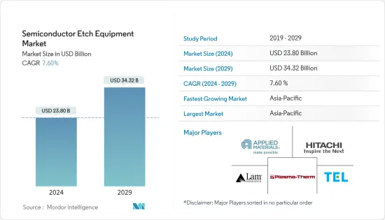
預計2024年全球半導體蝕刻設備市場規模將達238億美元,2024-2029年預測期間複合年成長率為7.60%,2029年將達343.2億美元。
主要亮點
- 蝕刻是半導體製造週期中的關鍵製程之一。該過程從半導體表面去除材料並為應用創建圖案。半導體蝕刻設備市場的成長高度依賴半導體晶圓沉積和晶圓加工產業的市場開拓。
- Lam Research 表示,人工智慧、5G 和物聯網等日益成長的長期推動因素是第一位的。此外,製造先進半導體裝置的複雜性持續快速增加,促使所有區隔市場的設備能力不斷增強。
- 許多大公司正在投資擴大其製造工廠。 2022 年 2 月,博世宣布有意擴建其位於德國羅伊特林根的晶圓製造工廠。到2025年,博世計畫斥資超過2.5億歐元(2.782億美元)擴大生產空間並建造必要的無塵室設施。這些擴張計劃正在推動半導體蝕刻設備市場的成長。
- 然而,半導體是廣泛交易的產品,具有複雜的製造供應鏈。過於複雜的海關和貿易程序、要求和做法可能會極大地擾亂半導體供應鏈,並造成代價高昂的壁壘,損害企業和消費者的利益。
- 由於COVID-19疫情爆發,該產業出現高額虧損和需求增加,導致供應鏈出現巨大缺口。由於擔心汽車等關鍵產業對晶片的需求下降,病毒最初的傳播導致晶圓代工廠關閉並降低了運轉率。儘管半導體代晶圓代工廠最初預測需求增加,但產量下降導致全球半導體短缺。
半導體蝕刻設備市場趨勢
導體蝕刻佔最大市場佔有率
- 導體蝕刻設備廣泛用於形成用於半導體裝置各部分的電激活材料。即使這些小型半導體結構中的微小變化也可能導致影響裝置性能的電氣缺陷。
- 對半導體電路小型化的需求不斷成長,以及批量生產具有微小缺陷的多層薄膜疊層的需求,預計將在預測期內推動各類導體蝕刻設備的需求增加。
- 導體蝕刻有助於在半導體裝置中形成電活性材料。即使這些微觀結構的微小變化也會降低裝置性能。此外,隨著DRAM晶片的需求不斷增加,許多公司正在引入導體蝕刻系統來大規模生產先進的DRAM。
- 例如,Applied Materials 的 Centris Sym3 Y 是最先進的導體蝕刻系統之一,專為 3D NAND、DRAM 和晶圓代工廠邏輯節點中的關鍵導體蝕刻應用而客製化。應用材料公司最先進的導體蝕刻設備專門用於 3D NAND、DRAM 和晶圓代工廠邏輯節點中的關鍵導體蝕刻應用。
- 此外,金屬-絕緣體-金屬(MIM)電容器中導體蝕刻應用的成長也是導體蝕刻的機會因素。 MIM 電容器是能源儲存、訊號濾波和高頻調諧應用的關鍵元件。
亞太地區正在經歷顯著成長
- 亞太地區在全球半導體晶圓代工廠中佔有最顯著的佔有率,主要企業有台積電和三星電子等。台灣、韓國、日本和中國大陸佔很大比例。
- 根據半導體產業協會2021年7月的調查顯示,中國已經掌握了多項晶片技術,商用半導體產業還比較年輕。儘管如此,中國政府仍在努力縮小差距,2014 年至 2030 年間在半導體領域投資超過 1,500 億美元。在蓬勃發展的市場和政府投資的支持下,中國預計將在某些半導體區隔市場變得更具競爭力。
- 此外,CNBC 於 2022 年 12 月報道稱,中國正在為其半導體行業製定價值超過 1 兆元美國(1,430 億美元)的一攬子支持計劃,標誌著朝著晶片自給自足邁出了重要一步。的技術進步。北京計劃推出預計將成為其最重要的財政激勵措施之一,在五年內分配,主要以補貼和稅額扣抵的形式,以促進國內半導體生產和研究活動。
- 日本政府也提供財政援助,鼓勵外國晶片製造商在日本建廠,為市場創造積極的成長前景。例如,2022年6月,日本經濟產業省將為台積電、索尼集團和日本半導體公司在熊本縣建造的半導體工廠提供高達4760億日元(35億美元)的補貼。Denso. 宣布計劃提供該工廠的總投資預計將達到約86億美元,其中日本政府將支持約40%的成本。
- 該地區其他國家也出現了類似的趨勢。例如,2022年2月,美國半導體設備製造商Lam Research在韓國製造了下一代半導體製造核心設備。這些高選擇性蝕刻機支援 Gate All around (GAA) 和 3D 沉積技術。預計它將在三星電子下一代記憶體和系統半導體的開發中發揮重要作用。
半導體蝕刻設備產業概況
由於有多家現有公司,半導體蝕刻設備市場競爭適度。本公司的品牌形象對該市場有重大影響。由於資本需求較高,新進入障礙較高,各大公司紛紛採取併購策略來擴大市場佔有率。該市場的主要企業包括應用材料公司、日立高新技術美國公司、泛林研究公司和東京電子有限公司。
2022 年 6 月,AlixLab 開發了原子層蝕刻間距分裂 (APS),這是一種製造高填充半導體元件的創新方法,消除了製造過程中的多個步驟。該公司表示,這種方法使零件更便宜並且使用更少的資源。該公司還宣布已完成瑞典隆德 ProNano RISE無塵室中原子層蝕刻 (ALE) 設備的連接。
2022 年 2 月,泛林集團宣布推出全新選擇性蝕刻產品線,利用突破性晶圓製造技術和新化學物質,支援晶片製造商開發環柵 (GAA) 電晶體結構。該公司的選擇性蝕刻產品線由Argos、Prevos和Selis三款新產品組成,在先進邏輯和儲存半導體解決方案的設計和製造方面具有強大的優勢。
其他福利:
- Excel 格式的市場預測 (ME) 表
- 3 個月分析師支持
目錄
第1章簡介
- 研究假設和市場定義
- 調查範圍
第2章調查方法
第3章執行摘要
第4章市場洞察
- 市場概況
- 產業吸引力-波特五力分析
- 供應商的議價能力
- 買方議價能力
- 新進入者的威脅
- 替代品的威脅
- 競爭公司之間敵對關係的強度
- COVID-19 市場影響評估
第5章市場動態
- 市場促進因素
- 增加半導體製程的資本投資
- 快速的技術進步與遷移
- 市場限制因素
- 貿易擔憂和半導體記憶體市場
第6章市場區隔
- 依產品類型
- 高密度蝕刻設備
- 低密度蝕刻設備
- 蝕刻膜類型
- 導體蝕刻
- 介電蝕刻
- 多晶矽蝕刻
- 依用途
- 晶圓代工廠
- MEMS
- 感應器
- 功率元件
- 依地區
- 北美洲
- 歐洲
- 亞太地區
- 其他地區
第7章 競爭形勢
- 公司簡介
- Applied Materials Inc.
- Hitachi High Technologies America, Inc.
- Lam Research Corporation
- Tokyo Electron Limited
- Plasma-Therm LLC
- Panasonic Corporation
- SPTS Technologies Limited(Orbotech)
- Suzhou Delphi Laser Co., Ltd
- ULVAC Inc.
第8章投資分析
第9章 市場機會及未來趨勢
The Semiconductor Etch Equipment Market size is estimated at USD 23.80 billion in 2024, and is expected to reach USD 34.32 billion by 2029, growing at a CAGR of 7.60% during the forecast period (2024-2029).
Key Highlights
- Etching is one of the vital processes in a semiconductor fabrication cycle. This process eliminates the material from the surface of the semiconductor to generate patterns based on its applications. The growth of the semiconductor etch equipment market is highly dependent on the development of the semiconductor wafer deposition and wafer processing industry.
- As per Lam Research, there is a strong demand for etch and other fab equipment owing to several factors, the first being the strengthening of secular tailwinds such as AI, 5G, and IoT. Also, the complexity of manufacturing advanced semiconductor devices continues to increase at a rapid rate, as per the organization, leading to a rise in equipment capacity across all market segments.
- Many major players are investing in the expansion of their fabrication plants. In February 2022, Bosch disclosed its intention to increase the size of its wafer production facility in Reutlingen, Germany. It plans to spend more than EUR 250 million (USD 278.2 million) by 2025 to build expanded production space and the necessary clean-room amenities. Such expansion plans are fueling the growth of the semiconductor etching equipment market.
- However, semiconductors are a widely traded commodity with a complicated manufacturing supply chain. Overly complex customs and trade procedures, requirements, and practices can dramatically disrupt semiconductor supply chains, causing costly barriers that harm businesses and consumers.
- Owing to the outbreak of COVID-19, the industry was riddled with a high deficit and increasing demand, which has led to a significant supply chain gap. The initial spread of the virus led to the shutting down or the reduction of foundry capacity utilization, fearing the decreasing demand for the chips across major sectors, like automotive. The diminished output led to a global shortage of semiconductors as the demand increased despite the initial estimates by semiconductor foundries.
Semiconductor Etch Equipment Market Trends
Conductor Etching to Hold the Largest Market Share
- Conductor etching equipment is used widely to shape the electrically activated materials used in different parts of the semiconductor device. Even a minimal variation in these small semiconductor structures can lead to an electrical fault impacting the device's performance.
- The increasing demand for miniaturization of semiconductor circuits is anticipated to catalyze the ever-increasing demand for different types of conductor etching equipment, along with the need for high production of multi-film stacks with a minor fault during the forecasted period.
- Conductor etching helps in shaping the electrically active materials of a semiconductor device. The presence of even a slight variation in these miniature structures can degrade device performance. Moreover, with the growing demand for DRAM chips, many players have introduced conductor etch systems for the volume production of advanced DRAMs.
- For instance, Centris Sym3 Y is one of the most advanced conductor etch systems by Applied Materials and is tailored to critical conductor etch applications in 3D NAND, DRAM, and foundry-logic nodes. It enables chipmakers to precisely pattern and shape ever-smaller features in state-of-the-art memory and logic chips.
- Moreover, the growth of usage of conductor etching in Metal Insulator Metal (MIM) capacitors also acts as an opportunity factor for Conductor Etching. MIM capacitors are important components for energy storage, signal filtering, and high-frequency tuning applications.
Asia-Pacific to Witness Significant Growth
- The Asia-Pacific region has the most prominent share of global semiconductor foundries, with major companies such as TSMC, Samsung Electronics, etc. Taiwan, South Korea, Japan, and China have a significant market share in the region.
- According to a survey conducted by the Semiconductor Industry Association in July 2021, China mastered several chip technologies, and its commercial semiconductor industry is still relatively young. Still, the Chinese government is trying to close the gap, investing more than USD 150 billion in semiconductors between 2014 and 2030. Supported by booming markets and these government investments, China is poised to become increasingly competitive in some semiconductor market segments.
- Moreover, as per a report by CNBC in December 2022, China is working on a more than CNY 1 trillion (USD 143 billion) support package for its semiconductor industry, in a major step toward self-sufficiency in chips and to counter the United States moves aimed at slowing its technological advances. Beijing has planned to roll out what is expected to be one of its most significant fiscal incentive packages, allocated over five years, mainly as subsidies and tax credits to strengthen semiconductor production and research activities at home.
- Also, Japan's government is offering financial aid to encourage foreign chip makers to build plants in Japan, which is creating a positive growth outlook for the market. For instance, in June 2022, Japan's Ministry of Economy, Trade and Industry (METI) announced plans to offer subsidies worth up to JPY 476 billion (USD 3.5 billion) for a semiconductor plant being built in Kumamoto Prefecture by Taiwan Semiconductor Manufacturing Co. (TSMC), Sony Group and Denso. Total investment in the plant was expected to reach around USD 8.6 billion, with Japan's government supporting about 40% of the costs.
- A similar trend has also been observed across other countries in the region. For instance, in February 2022, Lam Research, a US semiconductor equipment company, manufactured next-generation core equipment for semiconductor manufacturing in South Korea. These highly selective etching devices support Gate All Around (GAA) and 3D stacking technology. The new equipment is expected to play an important role in developing Samsung Electronics' next-generation memory and system semiconductors.
Semiconductor Etch Equipment Industry Overview
The Semiconductor Etch Equipment Market is moderately competitive owing to the presence of some established players. The brand identity associated with the companies has a major influence in this market. As the barrier for the new entrants is high in the market due to the high capital incorporated, major players are adopting mergers and acquisition strategies to gain more market share. Some major players operating in the market include Applied Materials Inc., Hitachi High Technologies America, Inc., Lam Research Corporation, and Tokyo Electron Limited.
In June 2022, AlixLab developed a new, innovative method for manufacturing semiconductor components with a high degree of packing, eliminating several steps in the manufacturing process - Atomic Layer Etch Pitch Splitting (APS). According to the company, the method makes the components cheaper and less resource-intensive. The company also announced the completion of the Atomic Layer Etch (ALE) equipment hook-up in its clean room at ProNano RISE in Lund, Sweden.
In February 2022, Lam Research Corp. announced a new suite of selective etch products that apply breakthrough wafer fabrication techniques and novel chemistries to support chipmakers in developing gate-all-around (GAA) transistor structures. Composed of three new products, Argos, Prevos, and Selis, the company's selective etch portfolio provides a powerful advantage in the design and manufacture of advanced logic and memory semiconductor solutions.
Additional Benefits:
- The market estimate (ME) sheet in Excel format
- 3 months of analyst support
TABLE OF CONTENTS
1 INTRODUCTION
- 1.1 Study Assumptions and Market Definition
- 1.2 Scope of the Study
2 RESEARCH METHODOLOGY
3 EXECUTIVE SUMMARY
4 MARKET INSIGHTS
- 4.1 Market Overview
- 4.2 Industry Attractiveness - Porter's Five Forces Analysis
- 4.2.1 Bargaining Power of Suppliers
- 4.2.2 Bargaining Power of Buyers
- 4.2.3 Threat of New Entrants
- 4.2.4 Threat of Substitute Products
- 4.2.5 Intensity of Competitive Rivalry
- 4.3 Assessment of the Impact of COVID-19 on the Market
5 MARKET DYNAMICS
- 5.1 Market Drivers
- 5.1.1 Increase in Capital Spending on Semiconductor Processing
- 5.1.2 Rapid Technological Advances and Transition
- 5.2 Market Restraints
- 5.2.1 Trade Uncertainties and Semiconductor Memory Markets
6 MARKET SEGMENTATION
- 6.1 By Product Type
- 6.1.1 High-density Etch Equipment
- 6.1.2 Low-density Etch Equipment
- 6.2 By Etching Film Type
- 6.2.1 Conductor Etching
- 6.2.2 Dielectric Etching
- 6.2.3 Polysilicon Etching
- 6.3 By Application
- 6.3.1 Foundries
- 6.3.2 MEMS
- 6.3.3 Sensors
- 6.3.4 Power Devices
- 6.4 By Geography
- 6.4.1 North America
- 6.4.2 Europe
- 6.4.3 Asia-Pacific
- 6.4.4 Rest of the World
7 COMPETITIVE LANDSCAPE
- 7.1 Company Profiles
- 7.1.1 Applied Materials Inc.
- 7.1.2 Hitachi High Technologies America, Inc.
- 7.1.3 Lam Research Corporation
- 7.1.4 Tokyo Electron Limited
- 7.1.5 Plasma-Therm LLC
- 7.1.6 Panasonic Corporation
- 7.1.7 SPTS Technologies Limited (Orbotech)
- 7.1.8 Suzhou Delphi Laser Co., Ltd
- 7.1.9 ULVAC Inc.
8 INVESTMENT ANALYSIS
9 MARKET OPPORTUNITIES AND FUTURE TRENDS
 2024 年蝕刻機世界市場報告
 半導體乾蝕蝕系統市場 - 2024 年至 2029 年預測
 2024-2032 年半導體介質蝕刻設備市場報告(按類型(濕蝕刻設備、乾蝕刻設備)、應用(鑄造廠、整合裝置製造商 (IDM))和地區
 半導體蝕刻設備市場報告:2030 年趨勢、預測與競爭分析
 蝕刻製程市場報告:2030 年趨勢、預測與競爭分析
 銅鈦蝕刻解決方案市場報告:2030 年趨勢、預測與競爭分析
 高純度蝕刻氣體市場報告:2030 年趨勢、預測與競爭分析
 半導體蝕刻設備全球市場規模、佔有率和行業趨勢分析報告:2023-2030年按類型、製程、最終用戶和地區分類的展望和預測
 2023-2030 年全球蝕刻化學品市場規模研究與預測(依最終用途產業、類型、應用和區域分析)
 半導體介質蝕刻設備市場報告:2030 年趨勢、預測與競爭分析