


 |
市場調查報告書
商品編碼
1404414
晶圓清洗設備:市場佔有率分析、產業趨勢與統計、2024年至2029年成長預測Wafer Cleaning Equipment - Market Share Analysis, Industry Trends & Statistics, Growth Forecasts 2024 - 2029 |
||||||
※ 本網頁內容可能與最新版本有所差異。詳細情況請與我們聯繫。
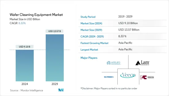
晶圓清洗設備市場規模預計到2024年為91億美元,預計到2029年將達到135.7億美元,在預測期內(2024-2029年)複合年成長率為8.33%。
晶圓清洗設備被用於無數的應用中,由於應用範圍的擴大對電子元件的巨大需求,高度回收電子封裝的措施正在增加。
主要亮點
- 智慧、相容設備和支援網路的日益普及是晶圓清洗設備全球市場開拓的主要驅動力。例如,2022 年 6 月,DISH 宣布將 Project Genesis 擴展到超過 20% 的美國人口(全國 120 個城市),僅在首次推出42 天後。因此,FCC 的暫定最後期限已經到來。此網路高度發達,完全雲端原生,並依賴開放的RAN架構。
- 此外,印刷電子的普及以及半導體裝置產業對升級和提高半導體產品品質和生產標準的興趣日益濃厚,也是支撐晶圓清洗設備市場發展的突出因素。
- 2022年6月,NEO Battery Materials Ltd.與一家生產印刷電路基板的韓國公司Automobile &PCB Inc.簽署了戰略合作備忘錄(MoU)。透過此次合作,兩家公司將利用 NEO 的技術專長以及 A&P 附屬公司 YSP 和 Yongsan 的既定網路來加強 NEO 的全球業務網路。此類產品開拓活動可以進一步推動印刷電子產品的成長,並創造市場開拓研究的需求。
- 預計對矽基感測器的需求不斷成長將為市場擴張提供良好的前景。此外,一些供應商已經在努力增加 SiC 晶圓的產量。例如,2023年8月,英飛凌科技股份公司宣布計劃擴建其在馬來西亞的製造工廠,並建立一座200毫米碳化矽工廠。這些發展顯示對晶圓遷移的需求不斷成長。
- 此外,Cree (Wolfspeed) 也正在提高 Wolfspeed 品牌的功率和射頻半導體的產能,這是該公司出售照明業務以專注於 SiC 和 GaN 產品時持續擴張的策略的一部分。為了滿足電動車、工業市場和行動通訊的高需求,Cree 正在紐約建造一座耗資 12 億美元的 200 毫米晶圓廠,預計將於 2022 年開始生產。
- 生產此類材料的一個主要挑戰是環境管理。晶圓清洗過程尤其會產生灰塵和生物危害廢棄物,如果處理不當,會對氣候產生直接影響。因此,政府制定了各種法規來考慮如何處理以避免此類問題。此外,對熟練勞動力的需求以及嚴格且不斷變化的品質標準正在阻礙市場成長。
晶圓清洗設備市場趨勢
智慧型手機和平板電腦推動市場成長
- 智慧型手機和平板電腦等家用電子電器的使用不斷增加正在刺激晶圓清洗設備市場的成長。新技術的出現以及消費者對更先進智慧型手機和平板電腦不斷成長的需求正在顯著推動行業成長的步伐。例如,愛立信預計,到 2027 年,全球智慧型手機用戶數量預計將達到 78.4 億。
- 由於平板電腦和智慧型手機市場的快速成長,對半導體晶圓的需求不斷增加,對晶圓清洗設備的需求也不斷增加。據印度蜂窩與電子協會 (ICEA) 稱,到 2025 年,印度筆記型電腦和平板電腦製造業的產值預計將達到 1,000 億美元。此外,到 2026 會計年度,印度行動電話市場的銷售額預計將達到 2.4 兆印度盧比(293.8 億美元)。
- 現在,電子郵件、社群媒體、遊戲和聊天等大多數任務都可以在智慧型手機上完成,因此對智慧型手機的需求不斷增加,而個人電腦銷售卻在下降。據 GSMA 稱,到 2025 年,將有約 75 億部連網智慧型手機,佔行動連線的五分之四以上。
- 智慧型手機技術正在開拓消費者的日常行銷策略、商業活動和生活方式。智慧型手機技術的接受程度是當今該技術成功的關鍵因素。因此,確定影響消費者對智慧型手機技術行為的關鍵因素具有重要價值。
- 根據 IBEF 報導,三星已宣布計劃未來五年在印度投資 3.7 兆印度盧比(500 億美元)用於製造行動電話。它還計劃根據 PLI 計劃生產價值超過 15,000 印度盧比(200 美元)的行動電話,價值 2.2 億印度盧比(300 億美元)。智慧型手機和平板電腦等家用電器的擴張可能會進一步提振對晶圓清洗設備的需求。
亞太地區正在經歷顯著的市場成長
- 亞太地區已成為最大的半導體市場。數位技術的滲透、快速的都市化和工業化正在推動這一成長。此外,大規模半導體製造、封裝和組裝產業的存在也為該地區晶圓設備市場的開拓創造了有利的前景。
- 此外,中國不僅是亞太地區,也是全球最大的半導體中心。根據半導體產業協會的數據,中國近期以1,925億美元的晶片銷售額領先半導體市場,與前一年同期比較去年同期成長27.1%。該國還吸引了主要晶片製造商的大量投資,透過建立新設施來擴大晶片生產。此外,WSTS 預測 2022 年全球銷售額將達到 5,730 億美元。
- 此外,在電動車產業需求不斷成長的推動下,日本企業正在大力投資以提高碳化矽功率半導體的產量。例如,總部位於東京的昭和電工公司於 2022 年 3 月開始量產直徑 6 吋(150 毫米)的碳化矽結晶晶圓(SiC 晶圓)。該晶圓將用作SiC磊晶晶圓的材料,該晶圓將被加工並安裝在SiC功率半導體上。
- 由於消費性電子和半導體產業不斷成長,亞太地區是重要的半導體晶圓清洗市場之一。對小型智慧移動設備的需求不斷成長正在支持該地區的市場成長。 IBEF 表示,印度消費電子 (ACE) 市場將以 9% 的複合年成長率成長,到 2022 年將達到 3.15 兆印度盧比(483.7 億美元)。此外,2022年9月,印度月度行動電話出口額首次突破10億美元大關。
- 冠狀病毒引發的居家趨勢大流行推動對半導體晶片的需求。例如,根據WSTS預測,2023年亞太地區半導體產業收入預計將超過4,000億美元。這些趨勢正在鼓勵主要設備製造商進入亞太市場。
- 例如,該市場最著名的供應商之一 ASML 最近在台灣台南開設了一個最先進的培訓設施。該地區的這種擴張可能會在預測期內進一步創造對晶圓清洗設備的需求。
晶圓清洗設備產業概況
晶圓清洗設備市場高度分散,主要企業包括 Lam Research Corporation、Applied Materials, Inc.、Veeco Instruments Inc.、Tokyo Electron Limited、Entegris, Inc、Modutek Corporation 和 Semes。這些參與企業佔有很大的佔有率並且高度可靠,從而導致市場整合。
- 2022年12月-SCREEN Holdings集團旗下SCREEN Semiconductor Solutions完成了單晶圓清洗設備「SU-3400」的開發,吞吐量為2,具有獨特的清洗技術。
- 2022 年 12 月 - 東京威力科創 (Tokyo Electron) 宣布推出 CELLESTA MS2,這是一種表面處理和晶圓清洗系統,配備雙流體噴霧技術和使用刷子的物理清洗功能。該設備能夠同時清洗晶圓的兩面,當需要清洗晶圓的兩面時,單位面積的生產率比我們傳統設備增加1.5倍以上。
其他福利
- Excel 格式的市場預測 (ME) 表
- 3 個月分析師支持
目錄
第1章簡介
- 研究成果
- 研究場所
- 調查範圍
第2章調查方法
第3章執行摘要
第4章市場動態
- 市場概況
- 市場促進因素與市場抑制因素簡介
- 市場促進因素
- 平板電腦和智慧型手機的需求不斷成長
- 半導體產業的成長
- 市場抑制因素
- 與晶圓清洗過程中產生的危險化學品和氣體相關的環境問題
- 產業價值鏈分析
- 產業吸引力-波特五力分析
- 新進入者的威脅
- 買方議價能力
- 供應商的議價能力
- 替代品的威脅
- 競爭公司之間的敵對關係
第5章技術概況
- 單晶圓噴塗系統
- 單晶圓低溫系統
- 批量浸泡式清洗系統
- 批量噴淋清洗系統
- 洗滌器
第6章市場區隔
- 依運轉模式類型
- 自動化設備
- 半自動設備
- 手動裝置
- 按用途
- 智慧型手機和平板電腦
- 記憶設備
- 射頻裝置
- LED
- 其他
- 按地區
- 北美洲
- 美國
- 加拿大
- 歐洲
- 德國
- 法國
- 義大利
- 英國
- 歐洲其他地區
- 亞太地區
- 中國
- 日本
- 台灣
- 韓國
- 其他亞太地區
- 其他
- 北美洲
第7章競爭形勢
- 公司簡介
- Applied Materials, Inc.
- Lam Research Corporation
- Veeco Instruments Inc.
- Screen Holdings Co., Ltd
- Modutek Corporation
- Entegris, Inc
- PVA Tepla AG
第8章投資分析
第9章市場的未來
The Wafer Cleaning Equipment Market size is estimated at USD 9.10 billion in 2024, and is expected to reach USD 13.57 billion by 2029, growing at a CAGR of 8.33% during the forecast period (2024-2029).
Due to the massive demand for electronic components owing to amplified usage, the increasing measures to make electronic packaging highly resourceful have made wafer-cleaning equipment used in myriad applications.
Key Highlights
- The growth in adopting smart and compatible devices and feasible networks is significantly aiding the development of the global wafer-cleaning equipment market. For instance, in June 2022, DISH informed that Project Genesis would be expanded to over 20% of the US population (in 120 cities across the USA) only 42 days after the initial launch. As such, it just met the FCC's interim deadline. The network is very developed, completely cloud-native, and reliant on Open RAN architecture.
- Furthermore, the increasing penetration of printed electronics and rising concern for upgrading and improving the semiconductor product quality and production standards in the semiconductor devices industry are some prominent factors behind the development of the Wafer Cleaning Equipment Market.
- In June 2022, NEO Battery Materials Ltd. signed a strategic Memorandum of Understanding (MoU) with Automobile & PCB Inc., a Korean company manufacturing printed circuit boards. Through this collaboration, both players will leverage NEO's technical expertise and the reputable and recognized network of A&P's related companies, YSP and Yongsan, to strengthen NEO's business network globally. Such activities for product development may further drive the growth of printed electronics, creating demand for studied market growth.
- An increase in demand for silicon-based sensors is anticipated to deliver lucrative possibilities for market expansion. Further, some vendors are already working toward increasing the production of SiC wafers. For instance, in August 2023, Infineon Technologies AG announced its plans to expand its manufacturing facility in Malaysia to establish 200 mm SiC fab. Such developments indicate the growing demand for wafer transition.
- Furthermore, Cree (Wolfspeed) is also elevating its production capacity for its Wolfspeed brand of power and radio frequency semiconductors, an ongoing strategy that grew when the company sold its lighting business to focus on SiC and GaN products. To meet the high demand in EVs, industrial markets, and mobile telecommunications, Cree is building a USD 1.2 billion 200mm SiC wafer fab in New York, where production began in 2022.
- The major challenge for the production of these materials is to control the environment, especially in the process of wafer cleaning, especially dust and biohazard waste are generated, which have a direct impact on the climate if they are not appropriately treated. Therefore different government regulations are made to consider how they must be handled to avoid such problems. Moreover, the need for a skilled workforce and strict and changing quality standards hinder the market growth.
Wafer Cleaning Equipment Market Trends
Smartphones & Tablets to Drive the Market Growth
- The increase in the usage of consumer electronic devices such as smartphones and tablets has stimulated the growth of the wafer-cleaning equipment market. Emerging new technologies and growth in consumer demand for more advanced smartphones and tablets have boosted the growth pace of the industry to a great extent. For instance, according to Ericsson, the global number of smartphone subscribers is anticipated to reach 7,840 million by 2027.
- The enormous growth in the tablets and smartphones market has raised the need for semiconductor wafers, thus raising the demand for wafer-cleaning equipment. According to India Cellular & Electronics Association (ICEA), India is anticipated to acquire a value of USD 100 billion in manufacturing laptops and tablets by 2025. In addition, the Indian mobile phone market is expected to generate INR 2.4 trillion (USD 29.38 billion) in revenue by FY2026.
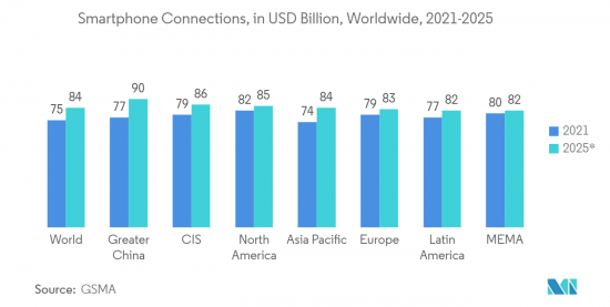
- The demand for smartphones has increased, and PC sales have declined because most tasks, such as emailing, social media, gaming, and chatting, can now be done via smartphones. According to GSMA, there will be about 7.5 billion smartphone connections by 2025, accounting for above four in five mobile connections.
- Smartphone technology is developing to influence the consumer's daily marketing strategies, business activities, and lifestyle. The acceptance of smartphone technology is a crucial factor in the success of today's technology. Due to this, identifying the main factors that influence the consumer's behavior toward smartphone technology is extremely valuable.
- According to IBEF, Samsung announced plans to invest INR 3.7 lakh crore (USD 50 billion) in India over the next five years to manufacture phones. It plans to produce phones worth INR 2.2 lakh crore (USD 30 billion), priced above INR 15,000 (USD 200), under the PLI scheme. Such expansion in consumer electronics such as smartphones and tablets may further drive the demand for Wafer Cleaning equipment.
Asia Pacific to Experience Significant Market Growth
- Asia Pacific region has appeared as the largest semiconductor market. The growing penetration of digital technologies, rapid urbanization, and industrialization contribute to this growth. Additionally, the presence of large semiconductor manufacturing, packaging, and assembly industries also creates a favorable scenario for developing the wafer equipment market in the region.
- In addition, China is the largest semiconductor hub not only in Asia-Pacific but also in the world. As per Semiconductor Industry Association, China recently led the semiconductor market with total chip sales of USD 192.5 billion, marking an expansion of 27.1 percent year on year. The country also draws huge investments from significant chipmakers to extend chip production by launching new facilities. Further, in 2022, WSTS forecasted global sales totaled USD 573 billion.
- Furthermore, Japanese companies are creating heavy investments to improve the production of SiC power semiconductors driven by the increased demand from the EV industry. For instance, in March 2022, Tokyo-headquartered Showa Denko KK introduced the mass production of silicon carbide single crystal wafers (SiC wafers) with a diameter of 6 inches (150 mm), which are used as materials for SiC epitaxial wafers to be processed and installed into SiC power semiconductors.
- Asia-Pacific is one of the vital semiconductor wafer cleaning markets owing to the presence of the ever-growing consumer electronics and semiconductor industries. The rise in demand for small and smart portable devices supplements the market growth in the region. According to IBEF, India's consumer electronics (ACE) market increased at 9 percent CAGR to reach INR 3.15 trillion (USD 48.37 billion) in 2022. Furthermore, in September 2022, monthly mobile phone exports from India crossed the USD 1 billion mark for the first time.
- The stay-at-home trend spurred by the coronavirus pandemic continues to drive the demand for semiconductor chips. For instance, according to WSTS, the estimated semiconductor industry revenue in the Asia Pacific region is expected to reach over USD 400 billion in 2023. Such trends encourage leading equipment manufacturers to enter the Asia Pacific (APAC) market.
- For instance, ASML, one of the most prominent vendors in the market, recently opened a new state-of-the-art training facility in Tainan, Taiwan. The above expansion in the region may further create demand for the Wafer Cleaning Equipment in the forecasted period.
Wafer Cleaning Equipment Industry Overview
The Wafer Cleaning Equipment Market is quite fragmented, with the major players in the studied market such as Lam Research Corporation, Applied Materials, Inc., Veeco Instruments Inc., Tokyo Electron Limited, Entegris, Inc, Modutek Corporation, Semes Co., Ltd., among others. These players account for a significant share and are reliable, leading to higher market consolidation.
- December 2022 - SCREEN Semiconductor Solutions Co., Ltd., a SCREEN Holdings Group company, finalized the development of its new SU-3400 single-wafer cleaning system, which provides throughput2 and a range of unique cleaning technologies.
- December 2022 - Tokyo Electron announced the launch of the CELLESTA MS2, a system for surface preparation and wafer cleaning, which incorporates a physical cleaning function featuring dual-fluid spray technology and brushes. Its capability to process both wafer sides simultaneously significantly boosts the system's productivity per unit area, pushing it over 1.5 times more productive than TEL's existing systems when both wafer sides need to be cleaned.
Additional Benefits:
- The market estimate (ME) sheet in Excel format
- 3 months of analyst support
TABLE OF CONTENTS
1 INTRODUCTION
- 1.1 Study Deliverables
- 1.2 Study Assumptions
- 1.3 Scope of the Study
2 RESEARCH METHODOLOGY
3 EXECUTIVE SUMMARY
4 MARKET DYNAMICS
- 4.1 Market Overview
- 4.2 Introduction to Market Drivers and Restraints
- 4.3 Market Drivers
- 4.3.1 Growing Demand for Tablets and Smartphones
- 4.3.2 Growth in the Semiconductor Industry
- 4.4 Market Restraints
- 4.4.1 Environmental Concerns Related to Hazardous Chemicals and Gases Generated During Wafer Cleaning Process
- 4.5 Industry Value Chain Analysis
- 4.6 Industry Attractiveness - Porter's Five Forces Analysis
- 4.6.1 Threat of New Entrants
- 4.6.2 Bargaining Power of Buyers
- 4.6.3 Bargaining Power of Suppliers
- 4.6.4 Threat of Substitute Products
- 4.6.5 Intensity of Competitive Rivalry
5 TECHNOLOGY SNAPSHOT
- 5.1 Single-wafer Spray Systems
- 5.2 Single-wafer Cryogenic Systems
- 5.3 Batch Immersion Cleaning Systems
- 5.4 Batch Spray Cleaning Systems
- 5.5 Scrubbers
6 MARKET SEGMENTATION
- 6.1 By Operating Mode Type
- 6.1.1 Automatic Equipment
- 6.1.2 Semi-automatic Equipment
- 6.1.3 Manual Equipment
- 6.2 By Application
- 6.2.1 Smartphones & Tablets
- 6.2.2 Memory Devices
- 6.2.3 RF Device
- 6.2.4 LED
- 6.2.5 Other Applications
- 6.3 By Geography
- 6.3.1 North America
- 6.3.1.1 United States
- 6.3.1.2 Canada
- 6.3.2 Europe
- 6.3.2.1 Germany
- 6.3.2.2 France
- 6.3.2.3 Italy
- 6.3.2.4 United Kingdom
- 6.3.2.5 Rest of Europe
- 6.3.3 Asia Pacific
- 6.3.3.1 China
- 6.3.3.2 Japan
- 6.3.3.3 Taiwan
- 6.3.3.4 South Korea
- 6.3.3.5 Rest of the Asia Pacific
- 6.3.4 Rest of the World
- 6.3.1 North America
7 COMPETITIVE LANDSCAPE
- 7.1 Company Profiles
- 7.1.1 Applied Materials, Inc.
- 7.1.2 Lam Research Corporation
- 7.1.3 Veeco Instruments Inc.
- 7.1.4 Screen Holdings Co., Ltd
- 7.1.5 Modutek Corporation
- 7.1.6 Entegris, Inc
- 7.1.7 PVA Tepla AG
8 INVESTMENT ANALYSIS
9 FUTURE OF THE MARKET
 晶圓清洗設備的全球市場:2023年
 全球晶圓清洗設備市場-全球產業規模、佔有率、趨勢、機會、預測,全球晶圓清洗設備市場按設備類型、晶圓尺寸、功能、應用、地區、預測和機會細分,2018-2028
 晶圓清洗設備全球市場規模、佔有率和產業趨勢分析報告:2023-2030年按設備類型、應用、晶圓尺寸、地區分類的展望與預測
 晶圓清洗設備的全球市場:按設備類型、按用途、按技術、按操作模式、按晶圓尺寸、按地區 - 預測到 2028 年
 全球半導體晶圓清洗設備市場
 晶圓清洗設備的全球市場
 晶圓清洗設備市場:按設備類型、尺寸、雜質、操作模式、用途- 2023-2030 年全球預測
 半導體晶圓清洗設備的全球市場:趨勢,機會,競爭分析(2023年~2028年)
 時鐘抖動清潔器的全球市場調查報告-產業分析,規模,佔有率,成長,趨勢,2022年~2028年前的預測
 全球半導體晶圓清洗設備市場:增長、未來展望、競爭對手分析(2022-2030)