


 |
市場調查報告書
商品編碼
1433754
半導體CVD設備:市場佔有率分析、產業趨勢/統計、成長預測(2024-2029)Semiconductor CVD Equipment - Market Share Analysis, Industry Trends & Statistics, Growth Forecasts (2024 - 2029) |
||||||
※ 本網頁內容可能與最新版本有所差異。詳細情況請與我們聯繫。
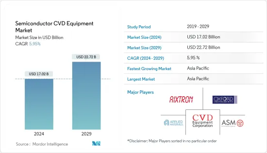
半導體CVD設備市場規模預計到2024年為170.2億美元,預計到2029年將達到227.2億美元,在預測期內(2024-2029年)複合年成長率為5.95%。
由於對基於微電子的消費產品的需求不斷增加,半導體、LED 和儲存設備行業的快速成長,以及對電鍍用 Cr6 的嚴格規定,主要推動了 CVD 設備市場的成長。
主要亮點
- 化學氣相沉積(CVD)製程常用於半導體製造和薄膜製造。近年來,隨著2D材料無機薄膜和可共形沉澱到各種基板上的高純度聚合物薄膜的精密製造,CVD合成已達到新的高度。
- 在半導體化學氣相沉積系統中,前驅氣體(通常用載氣稀釋)在接近室溫的常溫下供應到反應室。這些氣體在穿過或接觸加熱的基板時會發生反應或分解,產生沉積在基板上的固相。基板的溫度很重要,因為它會影響發生的反應。
- CVD 作為一種微加工技術被廣泛用於沉積各種型態的材料,包括多晶、結晶、非晶質和磊晶。這些材料包括矽(二氧化矽、碳化物、氮化物、氮氧化物)、碳(纖維、奈米纖維、奈米管、鑽石、石墨烯)、碳氟化合物、燈絲、鎢、氮化鈦和各種高k 電介質。
- 政府和相關人員正在密切關注微電子產業的發展,因為這些技術有可能顛覆和推動物聯網市場。隨著虛擬實境和擴增實境設備的採用增加,微電子研究和開發也可能增加,以應對迫在眉睫的頻寬限制。
- 他們製造半導體。設定 CVD 既複雜又昂貴。隨著晶圓代工廠和半導體封裝測試公司(OSAT)繼續擴大產量以滿足不斷成長的晶片需求,資本支出壓力可能會增加。
- COVID-19的疫情從需求和供應雙方影響了整個半導體和晶片製造市場。全國各地半導體工廠停工、倒閉,進一步加劇了供不應求的趨勢。然而,這些影響可能是短期的,並且對 CVD 技術的需求產生暫時的影響。此外,世界各國政府為支持汽車和工業部門所採取的預防措施可能有助於重振晶圓代工廠業的成長。
半導體CVD市場趨勢
微電子和消費性電子產品需求不斷成長推動需求
- 微電子和消費性電子產品銷售的增加預計將在預測期內推動半導體 IC 需求。然而,半導體IC的需求預計將增加半導體裝置製造商的產能,這可能會增加化學氣相沉積市場的需求。
- 整合設備製造商 (IDM) 包括邏輯元件、光電子元件、感測器、分立元件等。 (不包括記憶製造商)。整合設備製造商生產和銷售積體電路 (IC)。典型的 IDM 擁有自有品牌晶片,在內部設計並在製造工廠製造。雖然 IDM 追求從 10nm 到 5nm 甚至 3nm 的節點縮放,但其他製造商正在放棄平面架構,轉而採用複雜的邏輯和記憶體3D(3D) 結構。
- 薄膜形成是積體電路(IC)製造的重要步驟。最常見的薄膜生長方法是 CVD。在 CVD 中,前驅物和反應物在處理室中混合,然後在穩態條件下輸送以在晶圓上形成薄膜。
- 在市場競爭中,各IDMS都在採取各種措施來獲得競爭優勢。例如,加拿大光子製造中心(CPFC)是一家提供製造服務、預商用光子裝置和光子積體電路製造商的設施。 CPFC 提供的收費服務包括設計和建模、磊晶、製造、測試和表徵。 CPFC運作金屬有機化學氣相沉積(MOCVD)反應器,並研究製造砷化鎵(GaAs)和磷化銦(InP)基底元件。
- 政府和相關人員也密切關注微電子產業的進步,因為這些技術有可能顛覆和激發物聯網市場。由於虛擬實境和擴增實境(AR)設備的日益普及以及迫在眉睫的頻寬壓力,微電子研究和開發也可能會增加。 2021年9月,德國政府與歐洲和國際半導體產業的50名代表舉行會議,透過提出支持措施說服他們投資德國。德國政府計劃斥資約45億美元奪回整個半導體價值鏈的製造地。
全球半導體CVD設備最具優勢的市場是亞太地區。
- 亞太地區是一個具有潛力的地區,擁有各種製造設施,可用於開發家用電子電器和半導體相關產品。預計該地區將在未來幾年佔據半導體 CVD 設備市場的最大市場佔有率。
- 特別是,中國電子和半導體產業的發展正在支持該地區的市場擴張。在中國和印度等成長型經濟體中,工業化程度的提高以及最終用戶部門和公司數量的擴張開闢了巨大的未開發潛力。由於新興經濟體的存在和電子工業的發展,預計該地區在預測期內將以相當快的速度發展。
- 中國有一個非常雄心勃勃的半導體議程。該國計劃在1500億美元的資金支持下發展國內積體電路產業並製造更多晶片。大中華區,包括香港、中國和台灣,是一個地緣政治熱點。美國之間的貿易戰進一步加劇了該地區的緊張局勢,該地區是主要工藝技術的發源地,迫使許多中國企業投資半導體晶圓代工廠。
- 電動車需求不斷成長預計將推動亞太地區汽車半導體產業的快速擴張。汽車製造商必須繼續創新、創造和開發自動駕駛汽車。自動駕駛汽車已經吸引了主要汽車製造國的許多客戶。
- 由於人口眾多,印度已成為世界上成長最快的經濟體之一。據預測,未來幾年該國汽車半導體市場將快速擴張。汽車產業得到了強大的半導體研發基礎設施的補充,印度半導體蝕刻市場很可能在未來幾年開闢新的可能性。
半導體CVD產業概況
市場分散,競爭企業之間的競爭非常激烈。由於競爭公司的市場滲透率和提供先進產品的能力,預計它們之間的敵意也會很高。儘管市場參與者眾多,但只有少數企業能夠以高標準、過硬的品質在市場上脫穎而出。
- 2021 年 8 月 - 化學氣相沉積設備領先供應商之一的 CVD 設備公司宣布,已訂單美國一家主要電動車電池材料製造商約 170 萬美元的生產系統訂單。該系統將於2022年第一季交付給客戶。
- 2021 年 7 月 - ASM International NV 推出 Intrepid ESATM磊晶設備,適用於功率和類比裝置以及磊晶矽晶圓中的 300mm 應用。這款新型 ESA 儀器是 ASM 首款 300mm 大氣星團儀器,基於經過驗證的生產 Intrepid 平台,增強了 ASM 的大氣磊晶能力。 Intrepid ESA 的晶圓性能。
其他福利:
- Excel 格式的市場預測 (ME) 表
- 3 個月分析師支持
目錄
第1章簡介
- 研究假設和市場定義
- 調查範圍
第2章調查方法
- 研究框架
- 二次調查
- 初步調查
- 對資料進行三角測量並產生見解
第3章執行摘要
第4章市場洞察
- 市場概況
- 產業吸引力-波特五力分析
- 供應商的議價能力
- 買方議價能力
- 新進入者的威脅
- 替代品的威脅
- 競爭公司之間的敵對關係
- 價值鏈分析
- COVID-19 市場影響評估
第5章市場動態
- 市場促進因素
- 對微電子和半導體裝置的需求增加
- 增加對多個最終用戶的技術應用
- 市場限制因素
- 技術投入高
- CVD 製程技術簡介
- 大氣壓力化學氣相沉積(APCVD)
- 密度等離子體化學氣相沉積 (dpcvd)
- 低壓化學氣相沉積 (LPCVD)
- 金屬有機化學氣相沉積(MOCVD)
第6章市場區隔
- 按用途
- 鑄造廠
- 整合設備製造商(IDM)
- 記憶體製造商
- 按地區
- 北美洲
- 歐洲
- 亞太地區
- 世界其他地區
第7章 競爭形勢
- 公司簡介
- Aixtron Se
- Applied Materials, Inc.
- Asm International
- Cvd Equipment Corporation
- Oxford Instruments Plc
- Lam Research Corporation
- Tokyo Electron Limited
- Ulvac Inc.
- Veeco Instruments Inc.
第8章 市場投資
第9章 市場機會及未來趨勢
The Semiconductor CVD Equipment Market size is estimated at USD 17.02 billion in 2024, and is expected to reach USD 22.72 billion by 2029, growing at a CAGR of 5.95% during the forecast period (2024-2029).
Increasing demand for microelectronics-based consumer products, resulting in the faster growth of the semiconductor, LED, and storage device industry and strict regulations on the use of Cr6 for electroplating are primarily driving the growth of the CVD equipment market.
Key Highlights
- The Chemical Vapor Deposition (CVD) process is often used in manufacturing semiconductors and producing thin films. In recent years, CVD synthesis has reached new heights with the precise manufacturing of both inorganic thin films of 2D materials and high-purity polymeric thin films that may be conformally deposited on various substrates.
- Precursor gases (typically diluted in carrier gases) are supplied into the reaction chamber at around ambient temperatures in semiconductor chemical vapor deposition equipment. They react or break down when they pass across or come into touch with a heated substrate, generating a solid phase that is deposited on the substrate. The temperature of the substrate is important because it can influence the reactions that occur.
- CVD is widely used in microfabrication techniques to deposit materials in various morphologies, including polycrystalline, monocrystalline, amorphous, and epitaxial. Silicon (dioxide, carbide, nitride, oxynitride), carbon (fiber, nanofibers, nanotubes, diamond, and graphene), fluorocarbons, filaments, tungsten, titanium nitride, and a variety of high-k dielectrics are among these materials.
- Governments and business stakeholders are watching developments in the microelectronics industry closely because these technologies have the potential to disrupt and propel the Internet of Things market. Due to the increased adoption of virtual reality and augmented reality gadgets, R&D for microelectronics may also increase in response to the looming bandwidth constraint.
- They are making semiconductors. CVD setup can be complex and comes with huge costs. The foundries and Outsources Semiconductor Assembly and Test (OSAT) companies are likely to face increased pressure on capital expenditures as they continue to expand production to address the rising chip demand.
- The COVID -19 outbreak affected the overall semiconductor and chip fabrication market from the demand and supply sides. The nationwide lockdowns and closure of semiconductor plants have further fueled the supply shortage trend. However, these effects are likely to be short-term and temporarily affect the demand for CVD technologies. Moreover, government precautions globally to support automotive and industrial sectors could help revive foundry industry growth.
Semiconductor CVD Market Trends
Increase in Demand for Microelectronics and Consumer Electronics to Fuel the Demand
- The rise in microelectronics and consumer electronics sales is expected to drive the demand for semiconductor ICs over the forecasted period. However, the demand for semiconductor ICs is expected to increase the production capacity of semiconductor device manufacturers, which may augment the demand in the chemical vapor deposition market.
- The integrated device manufacturer (IDM) includes logic, optoelectronics, sensors, discrete components, and others. (Excluding Memory Manufacturers). An integrated device manufacturer manufactures and sells integrated circuits (ICs). A classic IDM owns its branded chips, designs them in-house, and makes them in a fabrication factory. IDMs pursue node scaling beyond 10 nm to 5 nm and even 3 nm, while other manufacturers renounce planar architectures favoring sophisticated, three-dimensional (3D) structures for logic and memory.
- Thin-film deposition is a vital step in manufacturing integrated circuits (ICs). The most common approach for thin-film growth is CVD. Precursors and reactants are combined in a process chamber before being delivered in a steady state to form a film on the wafer in CVD.
- The market is witnessing the presence of various IDMS undertaking different initiatives to gain a competitive advantage. For instance, the Canadian Photonics Fabrication Centre (CPFC) is a facility that provides fabrication services, pre-commercial photonic devices, and photonic integrated circuit manufacturers. Design and modeling, epitaxy, fabrication, and test and characterization are among the fee-based services provided by CPFC. CPFC operates a metal-organic chemical vapor deposition (MOCVD) reactor for the research and fabrication of gallium arsenide (GaAs) and indium phosphide (InP)-based devices.
- Also, governments and industry stakeholders are keenly following the advances in the microelectronics industry as these technologies might potentially disrupt and boost the Internet of Things market. R&D for microelectronics may also increase with the impending bandwidth crunch due to the improved penetration of virtual reality and augmented reality devices. In September 2021, the government organized a conference with 50 European and international semiconductor industry representatives to persuade them to invest in Germany by offering them a help package. The German government plans to spend roughly USD 4.5 billion to recapture manufacturing locations across the semiconductor value chain.
Asia Pacific as the Most Lucrative Market for Global Semiconductor CVD Equipment
- The Asia Pacific is a potential region with various manufacturing facilities for developing consumer electronics and semiconductor-related products. The particular region is expected to occupy the largest market share in the semiconductor CVD equipment market in the coming years.
- The advancement of the electronics and semiconductor industries, particularly in China, is driving market expansion in the region. In growing economies like China and India, the expansion in industrialization and the number of end-user sectors and companies presented enormous undiscovered potential. Due to the sheer existence of growing economies and the development of the electronics industries, the region is predicted to propel at a significant rate over the forecast period.
- China has a very ambitious semiconductor agenda. Backed by USD 150 billion in funding, the country is developing its domestic IC industry and plans to make more of its chips. Greater China, which encompasses Hong Kong, China, and Taiwan, is a geopolitical hotspot. The US-China trade war is compounding tensions in an area where all the leading process technology is located, forcing many Chinese companies to invest in their semiconductor foundries.
- The rapid expansion of the APAC automotive semiconductor industry is expected to be fueled by the rising demand for electric vehicles. Automobile manufacturers must continue to innovate, create, and develop self-driving cars, which have already attracted many customers in key automotive manufacturing countries.
- India has emerged as one of the world's fastest-growing economies due to its large population. According to projections, the automotive semiconductor market in the country will increase rapidly in the coming years. The Automotive industry is complemented by a strong semiconductor R&D infrastructure, which will open new potential for the semiconductor etch market in India in the forthcoming years.
Semiconductor CVD Industry Overview
The market is fragmented with high competitive rivalry. Also, owing to their market penetration and the ability to offer advanced products, the competitive rivalry is expected to be high. Although the market comprises various players, only a handful are prominent in the market for their high standards and excellent quality.
- August 2021 - CVD Equipment Corporation, one of the key suppliers of chemical vapor deposition systems, announced that it had secured a production system order worth about USD 1.7 million from a large US-based electric car battery material producer. In the first quarter of 2022, the system will be delivered to the customer.
- July 2021 - ASM International N.V. announced the availability of Intrepid ESATM epitaxy equipment for 300mm applications in power and analog devices and epitaxial silicon wafers. The new ESA tool increases ASM's atmospheric epi capabilities with ASM's first 300mm atmospheric cluster tool based on the proven, high-volume manufacturing Intrepid platform. On-wafer performance with the Intrepid ESA.
Additional Benefits:
- The market estimate (ME) sheet in Excel format
- 3 months of analyst support
TABLE OF CONTENTS
1 INTRODUCTION
- 1.1 Study Assumptions and Market Definition
- 1.2 Scope of the Study
2 RESEARCH METHODOLOGY
- 2.1 Research Framework
- 2.2 Secondary Research
- 2.3 Primary Research
- 2.4 Data Triangulation and Insight Generation
3 EXECUTIVE SUMMARY
4 MARKET INSIGHT
- 4.1 Market Overview
- 4.2 Industry Attractiveness - Porter's Five Forces Analysis
- 4.2.1 Bargaining Power of Suppliers
- 4.2.2 Bargaining Power of Buyers
- 4.2.3 Threat of New Entrants
- 4.2.4 Threat of Substitutes
- 4.2.5 Intensity of Competitive Rivalry
- 4.3 Value Chain Analysis
- 4.4 Assessment of Impact of Covid-19 on the Market
5 MARKET DYNAMICS
- 5.1 Market Drivers
- 5.1.1 Increase In Demand For Microelectronics And Semiconductor Devices
- 5.1.2 Rise In Application Of The Technology For Several End-users
- 5.2 Market Restraint
- 5.2.1 High Investment For The Technology
- 5.3 Cvd Processes Technology Snapshot
- 5.3.1 Atmospheric-pressure Chemical Vapor Deposition (apcvd)
- 5.3.2 Density-plasma Chemical Vapor Deposition (dpcvd)
- 5.3.3 Low-pressure Chemical Vapor Deposition (lpcvd)
- 5.3.4 Metal-organic Chemical Vapor Phase Deposition (mocvd)
6 MARKET SEGMENTATION
- 6.1 By Application
- 6.1.1 Foundry
- 6.1.2 Integrated Device Manufacturer (idm)
- 6.1.3 Memory Manufacturers
- 6.2 By Geography
- 6.2.1 North America
- 6.2.2 Europe
- 6.2.3 Asia-Pacific
- 6.2.4 Rest of The World
7 COMPETITIVE LANDSCAPE
- 7.1 Company Profiles
- 7.1.1 Aixtron Se
- 7.1.2 Applied Materials, Inc.
- 7.1.3 Asm International
- 7.1.4 Cvd Equipment Corporation
- 7.1.5 Oxford Instruments Plc
- 7.1.6 Lam Research Corporation
- 7.1.7 Tokyo Electron Limited
- 7.1.8 Ulvac Inc.
- 7.1.9 Veeco Instruments Inc.
8 MARKET INVESTMENTS
9 MARKET OPPORTUNITIES AND FUTURE TRENDS
 2024-2032 年化學氣相沉積設備市場報告(按技術(等離子體增強 CVD、低壓 CVD、金屬有機 CVD、常壓 CVD 等)、應用、最終用戶和地區)
 異質結 PECVD 設備市場報告:2030 年趨勢、預測與競爭分析
 金屬有機化學氣相沉積 (MOCVD) 市場報告:2030 年趨勢、預測與競爭分析
 2024 年 CVD(化學氣相沉積)全球市場報告
 CVD(化學氣相沉積)市場規模、佔有率、趨勢分析報告:2024-2030 年按類別、應用、地區和細分市場預測
 異質結(HJT)PECVD設備的全球市場:2023年
 化學氣相沉積 (CVD) 設備市場,按技術、按應用、按最終用戶、按國家和地區分類 - 2023-2030 年行業分析、市場規模、市場佔有率和預測
 電力電子用 MOCVD 設備的全球市場
 化學氣相沉積法的全球市場
 金屬有機氣相沉積 (MOCVD) 全球市場:應用/類別/區域分析、規模、趨勢、COVID-19 影響、到 2026 年預測